SDLS153A January 1981 – January 2016 SN74LS292 , SN74LS294
PRODUCTION DATA.
- 1 Features
- 2 Applications
- 3 Description
- 4 Revision History
- 5 Pin Configuration and Functions
- 6 Specifications
- 7 Parameter Measurement Information
- 8 Detailed Description
- 9 Application and Implementation
- 10Power Supply Recommendations
- 11Layout
- 12Device and Documentation Support
- 13Mechanical, Packaging, and Orderable Information
Package Options
Mechanical Data (Package|Pins)
- N|16
Thermal pad, mechanical data (Package|Pins)
Orderable Information
1 Features
2 Applications
- Frequency Division
- Digital Timing
3 Description
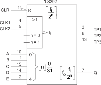
The SN74LS29x devices are programmable frequency dividers and digital timers contain 31 flip-flops plus 30 gates (in SN74LS292) or 15 flip-flops plus 29 gates (in SN74LS294) on a single chip. The count modulo is under digital control of the inputs provided.
Both types feature an active-low CLR clear input to initialize the state of all flip-flops. To facilitate the incoming inspection, test points are provided (TP1, TP2, and TP3 on the SN74LS292, and TP on the SN74LS294). These test points are not intended to drive system loads. Both types feature two clock inputs; either one may be used for clock gating (see Table 1).
A brief look at the digital timing capabilities of the SN74LS292 shows that with a 1-MHz input frequency, programming for 210 gives a period of 1.024 ms, 220 gives a period of 1.05 sec, 226 gives a period of 1.12 min, and 231 gives a period of 35.79 min.
These devices are easily cascadable, giving limitless possibilities to achievable timing delays.
Device Information(1)
| PART NUMBER | PACKAGE | BODY SIZE (NOM) |
|---|---|---|
| SN74LS292N | PDIP (16) | 6.35 mm × 19.30 mm |
| SN74LS294N |
- For all available packages, see the orderable addendum at the end of the data sheet.
Logic Symbols
