SDLS153A January 1981 – January 2016 SN74LS292 , SN74LS294
PRODUCTION DATA.
- 1 Features
- 2 Applications
- 3 Description
- 4 Revision History
- 5 Pin Configuration and Functions
- 6 Specifications
- 7 Parameter Measurement Information
- 8 Detailed Description
- 9 Application and Implementation
- 10Power Supply Recommendations
- 11Layout
- 12Device and Documentation Support
- 13Mechanical, Packaging, and Orderable Information
Package Options
Mechanical Data (Package|Pins)
- N|16
Thermal pad, mechanical data (Package|Pins)
Orderable Information
8 Detailed Description
8.1 Overview
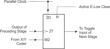
Functional Block Diagram shows that the count modulo is controlled by an X/Y decoder connected to the mode control inputs of several flip-flops. These flip-flops with mode controls each have a D input connected to the parallel clock line, and a T input driven by the preceding stage. The parallel clock frequency is always the input frequency divided by four.
The X/Y decoder output selected by the programming inputs goes low. While a mode control is slow, the D input of that flip-flop is enabled, and the signal from the parallel clock line (fin ÷ 4) is passed to the T input of the following stage. All the other mode controls are high, enabling the T inputs and causing each flip-flop in turn to divide by two.
8.2 Functional Block Diagram

8.3 Feature Description
This SN74LS29x device can be used to digitally program from 22 to 2n (n = 31 for SN74LS292, n = 15 for SN74LS294) divider chain. This has a useable frequency range up to 30 MHz. The flexibility is offered when the devices are cascaded to have desired timing delay.
8.4 Device Functional Modes
Table 1, Table 2, and Table 3 list the functional modes of the SN74LS292.
Table 1. Function Table
| CLEAR | CLK1 | CLK2 | Q OUTPUT MODE |
|---|---|---|---|
| L | X | X | Cleared to L |
| H | ↑ | L | Count |
| H | L | ↑ | Count |
| H | H | X | Inhibit |
| H | X | H | Inhibit |
Table 2. SN74LS292 Function Table
| PROGRAMMING INPUTS | FREQUENCY DIVISION | |||||||||||
|---|---|---|---|---|---|---|---|---|---|---|---|---|
| Q | TP1 | TP2 | TP3 | |||||||||
| E | D | C | B | A | BINARY | DECIMAL | BINARY | DECIMAL | BINARY | DECIMAL | BINARY | DECIMAL |
| L | L | L | L | L | Inhibit | Inhibit | Inhibit | Inhibit | Inhibit | Inhibit | Inhibit | Inhibit |
| L | L | L | L | H | Inhibit | Inhibit | Inhibit | Inhibit | Inhibit | Inhibit | Inhibit | Inhibit |
| L | L | L | H | L | 22 | 4 | 29 | 512 | 217 | 131072 | 224 | 16777216 |
| L | L | L | H | H | 23 | 8 | 29 | 512 | 217 | 131072 | 224 | 16777216 |
| L | L | H | L | L | 24 | 16 | 29 | 512 | 217 | 131072 | 224 | 16777216 |
| L | L | H | L | H | 25 | 32 | 29 | 512 | 217 | 131072 | 224 | 16777216 |
| L | L | H | H | L | 26 | 64 | 29 | 512 | 217 | 131072 | 224 | 16777216 |
| L | L | H | H | H | 27 | 128 | 29 | 512 | 217 | 131072 | 224 | 16777216 |
| L | H | L | L | L | 28 | 256 | 29 | 512 | 217 | 131072 | 22 | 4 |
| L | H | L | L | H | 29 | 512 | 29 | 512 | 217 | 131072 | 22 | 4 |
| L | H | L | H | L | 210 | 1024 | 29 | 512 | 217 | 131072 | 24 | 16 |
| L | H | L | H | H | 211 | 2048 | 29 | 512 | 217 | 131072 | 24 | 16 |
| L | H | H | L | L | 212 | 4096 | 29 | 512 | 217 | 131072 | 26 | 64 |
| L | H | H | L | H | 213 | 8192 | 29 | 512 | 217 | 131072 | 26 | 64 |
| L | H | H | H | L | 214 | 16384 | 29 | 512 | Disabled low | Disabled low | 28 | 256 |
| L | H | H | H | H | 215 | 32768 | 29 | 512 | Disabled low | Disabled low | 28 | 256 |
| H | L | L | L | L | 216 | 65536 | 29 | 512 | 23 | 8 | 210 | 1024 |
| H | L | L | L | H | 217 | 131072 | 29 | 512 | 23 | 8 | 210 | 1024 |
| H | L | L | H | L | 218 | 262144 | 29 | 512 | 25 | 32 | 212 | 4096 |
| H | L | L | H | H | 219 | 524288 | 29 | 512 | 25 | 32 | 212 | 4096 |
| H | L | H | L | L | 220 | 1048576 | 29 | 512 | 27 | 128 | 214 | 16384 |
| H | L | H | L | H | 221 | 2097152 | 29 | 512 | 27 | 128 | 214 | 16384 |
| H | L | H | H | L | 222 | 4194304 | Disabled low | Disabled low | 29 | 512 | 216 | 65536 |
| H | L | H | H | H | 223 | 8388608 | Disabled low | Disabled low | 29 | 512 | 216 | 65536 |
| H | H | L | L | L | 224 | 16777216 | 23 | 8 | 211 | 2048 | 218 | 262144 |
| H | H | L | L | H | 225 | 33554432 | 23 | 8 | 211 | 2048 | 218 | 262144 |
| H | H | L | H | L | 226 | 67108864 | 25 | 32 | 213 | 8192 | 220 | 1048576 |
| H | H | L | H | H | 227 | 134217728 | 25 | 32 | 213 | 8192 | 220 | 1048576 |
| H | H | H | L | L | 228 | 268435456 | 27 | 128 | 215 | 32768 | 222 | 4194304 |
| H | H | H | L | H | 229 | 536870912 | 27 | 128 | 215 | 32768 | 222 | 4194304 |
| H | H | H | H | L | 230 | 1073741824 | 29 | 512 | 217 | 131072 | 224 | 16777216 |
| H | H | H | H | H | 231 | 2147483648 | 29 | 512 | 217 | 131072 | 224 | 16777216 |
Table 3. SN74LS294 Function Table
| PROGRAMMING INPUTS | FREQUENCY DIVISION | ||||||
|---|---|---|---|---|---|---|---|
| Q | TP | ||||||
| D | C | B | A | BINARY | DECIMAL | BINARY | DECIMAL |
| L | L | L | L | Inhibit | Inhibit | Inhibit | Inhibit |
| L | L | L | H | Inhibit | Inhibit | Inhibit | Inhibit |
| L | L | H | L | 22 | 4 | 29 | 512 |
| L | L | H | H | 23 | 8 | 29 | 512 |
| L | H | L | L | 24 | 16 | 29 | 512 |
| L | H | L | H | 25 | 32 | 29 | 512 |
| L | H | H | L | 26 | 64 | 29 | 512 |
| L | H | H | H | 27 | 128 | Disabled Low | |
| H | L | L | L | 28 | 256 | 22 | 4 |
| H | L | L | H | 29 | 512 | 23 | 8 |
| H | L | H | L | 210 | 1024 | 24 | 16 |
| H | L | H | H | 211 | 2048 | 25 | 32 |
| H | H | L | L | 212 | 4096 | 26 | 64 |
| H | H | L | H | 213 | 8192 | 27 | 128 |
| H | H | H | L | 214 | 16384 | 28 | 256 |
| H | H | H | H | 215 | 32768 | 29 | 512 |
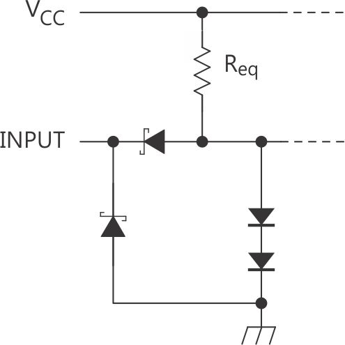
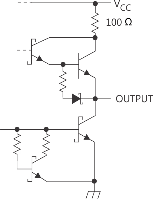
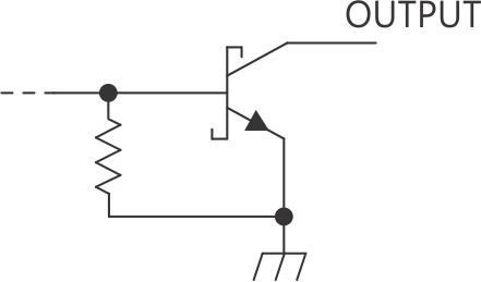
Figure 7, Figure 9, and Figure 9 show the schematics of inputs and outputs of the SN74LS292.
 Figure 7. Equivalent of Each Input
 Figure 8. Typical of Q Outputs
 Figure 9. Typical of TP Outputs