SCLS393Q APRIL 1998 – August 2015 SN74LV123A
UNLESS OTHERWISE NOTED, this document contains PRODUCTION DATA.
- 1 Features
- 2 Applications
- 3 Description
- 4 Revision History
- 5 Description (continued)
- 6 Pin Configuration and Functions
-
7 Specifications
- 7.1 Absolute Maximum Ratings
- 7.2 ESD Ratings
- 7.3 Recommended Operating Conditions
- 7.4 Thermal Information
- 7.5 Electrical Characteristics
- 7.6 Timing Requirements, VCC = 2.5 V ± 0.2 V
- 7.7 Timing Requirements, VCC = 3.3 V ± 0.3 V
- 7.8 Timing Requirements, VCC = 5 V ± 0.5 V
- 7.9 Switching Characteristics, VCC = 2.5 V ± 0.2 V
- 7.10 Switching Characteristics, VCC = 3.3 V ± 0.3 V
- 7.11 Switching Characteristics, VCC = 5 V ± 0.5 V
- 7.12 Operating Characteristics
- 7.13 Typical Characteristics
- 8 Parameter Measurement Information
- 9 Detailed Description
- 10Application and Implementation
- 11Power Supply Recommendations
- 12Layout
- 13Device and Documentation Support
- 14Mechanical, Packaging, and Orderable Information
Package Options
Mechanical Data (Package|Pins)
Thermal pad, mechanical data (Package|Pins)
- RGY|16
Orderable Information
1 Features
- 2-V to 5.5-V VCC Operation
- Maximum tpd of 11 ns at 5 V
- Typical VOLP (Output Ground Bounce)
< 0.8 V at VCC = 3.3 V, TA = 25°C - Typical VOHV (Output VOH Undershoot)
> 2.3 V at VCC = 3.3 V, TA = 25°C - Support Mixed-Mode Voltage Operation on
All Ports - Schmitt-Trigger Circuitry on A, B, and CLR Inputs for Slow Input Transition Rates
- Edge Triggered From Active-High or
Active-Low Gated Logic Inputs - Ioff Supports Partial-Power-Down Mode Operation
- Retriggerable for Very Long Output Pulses,
up to 100% Duty Cycle - Overriding Clear Terminates Output Pulse
- Glitch-Free Power-Up Reset on Outputs
- Latch-Up Performance Exceeds 100 mA Per JESD 78, Class 11
- ESD Protection Exceeds JESD 22
- 2000-V Human-Body Model (A114-A)
- 200-V Machine Model (A115-A)
- 1000-V Charged-Device Model (C101)
2 Applications
- AV Receivers
- Blu-ray Players and Home Theaters
- DVD Recorders and Players
- Desktop PCs or Notebook PCs
- Digital Radio and Internet Radio Players
- Digital Video Cameras (DVC)
- Embedded PCs
- GPS: Personal Navigation Devices
- Mobile Internet Devices
- Network Attached Storage (NAS)
- Personal Digital Assistant (PDA)
- Server PSU
- Solid-State Drive (SSD): Client and Enterprise
- Video Analytics Servers
- Wireless Headsets, Keyboard, and Mice
3 Description
The 'LV123A devices are dual retriggerable monostable multivibrators designed for 2-V to 5.5-V VCC operation.
Device Information(1)
| PART NUMBER | PACKAGE | BODY SIZE (NOM) |
|---|---|---|
| SN74LV123AD | SOIC (16) | 6.00 mm x 9.90 mm |
| SN74LV123ADB | SSOP (16) | 7.80 mm x 6.20 mm |
| SN74LV123ANS | SO (16) | 7.80 mm x 10.20 mm |
| SN74LV123APW | TSSOP (16) | 6.40 mm x 5.00 mm |
| SN74LV123ARGY | VQFN (16) | 3.50 mm x 4.00 mm |
- For all available packages, see the orderable addendum at the end of the data sheet.
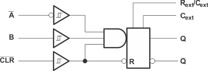
Logic Diagram, Each Multivibrator (Positive Logic)
