SCLS394J April 1999 – February 2015 SN74LV132A
PRODUCTION DATA.
- 1 Features
- 2 Applications
- 3 Description
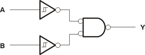
- 4 Logic Diagram (Positive Logic)
- 5 Revision History
- 6 Pin Configuration and Functions
-
7 Specifications
- 7.1 Absolute Maximum Ratings
- 7.2 ESD Ratings
- 7.3 Recommended Operating Conditions
- 7.4 Thermal Information
- 7.5 Electrical Characteristics
- 7.6 Switching Characteristics
- 7.7 Switching Characteristics
- 7.8 Switching Characteristics
- 7.9 Noise Characteristics for SN74LV132A
- 7.10 Operating Characteristics
- 7.11 Typical Characteristics
- 8 Parameter Measurement Information
- 9 Detailed Description
- 10Application and Implementation
- 11Power Supply Recommendations
- 12Layout
- 13Device and Documentation Support
- 14Mechanical, Packaging, and Orderable Information
Package Options
Refer to the PDF data sheet for device specific package drawings
Mechanical Data (Package|Pins)
- D|14
- DB|14
- DGV|14
- PW|14
- NS|14
Thermal pad, mechanical data (Package|Pins)
Orderable Information
1 Features
- 2-V to 5.5-V VCC Operation
- Max tpd of 9 ns at 5 V
- Typical VOLP (Output Ground Bounce) <0.8 V at VCC = 3.3 V, TA = 25°C
- Typical VOHV (Output VOH Undershoot) >2.3 V at VCC = 3.3 V, TA = 25°C
- Support Mixed-Mode Voltage Operation on All Ports
- Latch-Up Performance Exceeds 250 mA per JESD 17
- Ioff Supports Live Insertion, Partial Power-Down Mode, and Back Drive Protection
- ESD Protection Exceeds JESD 22
- 2000-V Human-Body Model (A114-A)
- 200-V Machine Model (A115-A)
- 1000-V Charged-Device Model (C101)
2 Applications
- Industrial PC: Rugged PC and Laptop
- Access Control and Security: Camera Surveillance IP Network
- Vending, Payment and Change Machines
- Patient Monitoring STB / DVR / Streaming Media (Withdraw)
- Other Motor Drives (Such as Switch Reluctance)
3 Description
The 'LV132A devices are quadruple positive-NAND gates designed for 2-V to 5.5-V VCC operation.
The 'LV132A devices perform the Boolean function Y = A • B or Y = A + B in positive logic.
Each circuit functions as a NAND gate, but because of the Schmitt trigger, it has different input threshold levels for positive- and negative-going signals.
These circuits are temperature compensated and can be triggered from the slowest of input ramps and still give clean jitter-free output signals.
Device Information(1)
| PART NUMBER | PACKAGE | BODY SIZE (NOM) |
|---|---|---|
| LV132A | SOIC (14) | 8.65 mm × 3.91 mm |
| SOP (14) | 10.30 mm × 5.30 mm | |
| SSOP (14) | 6.20 mm × 5.30 mm | |
| TSSOP (14) | 5.00 mm × 4.40 mm | |
| TVSOP (14) | 3.60 mm × 4.40 mm |
- For all available packages, see the orderable addendum at the end of the data sheet.
4 Logic Diagram (Positive Logic)