SCLS394J April 1999 – February 2015 SN74LV132A
PRODUCTION DATA.
- 1 Features
- 2 Applications
- 3 Description
- 4 Logic Diagram (Positive Logic)
- 5 Revision History
- 6 Pin Configuration and Functions
-
7 Specifications
- 7.1 Absolute Maximum Ratings
- 7.2 ESD Ratings
- 7.3 Recommended Operating Conditions
- 7.4 Thermal Information
- 7.5 Electrical Characteristics
- 7.6 Switching Characteristics
- 7.7 Switching Characteristics
- 7.8 Switching Characteristics
- 7.9 Noise Characteristics for SN74LV132A
- 7.10 Operating Characteristics
- 7.11 Typical Characteristics
- 8 Parameter Measurement Information
- 9 Detailed Description
- 10Application and Implementation
- 11Power Supply Recommendations
- 12Layout
- 13Device and Documentation Support
- 14Mechanical, Packaging, and Orderable Information
Package Options
Refer to the PDF data sheet for device specific package drawings
Mechanical Data (Package|Pins)
- D|14
- DB|14
- DGV|14
- PW|14
- NS|14
Thermal pad, mechanical data (Package|Pins)
Orderable Information
9 Detailed Description
9.1 Overview
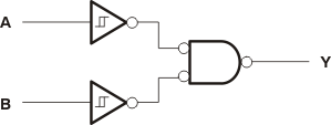
The SN74LV132A Is a quadruple 2-input positive NAND gate with low drive that produces slow rise and fall times. This reduces ringing on the output signal. Each circuit functions as a NAND gate, but because of the Schmitt trigger, it has different input threshold levels for positive- and negative-going signals. These circuits are temperature compensated and can be triggered from the slowest of input ramps and still give clean jitter-free output signals.
9.2 Functional Block Diagram
 Figure 4. Logic Diagram (Positive Logic)
9.3 Feature Description
- Wide operating voltage range, operates from 2 to 5.5 V
- Allows down voltage translation, inputs accept voltages to 5.5 V
9.4 Device Functional Modes
Table 1. Function Table
| INPUTS | OUTPUT Y |
|
|---|---|---|
| A | B | |
| H | H | L |
| L | X | H |
| X | L | H |