SCLS412K April 1998 – February 2023 SN74LV574A
PRODMIX
- 1 Features
- 2 Applications
- 3 Description
- 4 Revision History
- 5 Pin Configuration and Functions
-
6 Specifications
- 6.1 Absolute Maximum Ratings
- 6.2 ESD Ratings
- 6.3 Recommended Operating Conditions
- 6.4 Thermal Information
- 6.5 Electrical Characteristics
- 6.6 Timing Requirements, VCC = 2.5 V ± 0.2 V
- 6.7 Timing Requirements, VCC = 3.3 V ± 0.3 V
- 6.8 Timing Requirements, VCC = 5 V ± 0.5 V
- 6.9 Switching Characteristics, VCC = 2.5 V ± 0.2 V
- 6.10 Switching Characteristics, VCC = 3.3 V ± 0.3 V
- 6.11 Switching Characteristics, VCC = 5 V ± 0.5 V
- 6.12 Noise Characteristics
- 6.13 Operating Characteristics
- 6.14 Typical Characteristics
- 7 Parameter Measurement Information
- 8 Detailed Description
- 9 Application and Implementation
- 10Device and Documentation Support
- 11Mechanical, Packaging, and Orderable Information
Package Options
Refer to the PDF data sheet for device specific package drawings
Mechanical Data (Package|Pins)
- DGV|20
- DB|20
- NS|20
- DW|20
- PW|20
- RGY|20
Thermal pad, mechanical data (Package|Pins)
- RGY|20
Orderable Information
3 Description
The 'LV574A devices are octal edge-triggered D-type flip-flops designed for 2 V to 5.5 V VCC operation.
These devices feature 3-state outputs designed specifically for driving highly capacitive or relatively low-impedance loads. The devices are particularly suitable for implementing buffer registers, I/O ports, bidirectional bus drivers, and working registers.
On the positive transition of the clock (CLK) input, the Q outputs are set to the logic levels set up at the data (D) inputs.
| PART NUMBER | PACKAGE | BODY SIZE (NOM) |
|---|---|---|
| SN74LV574A | DB (SSOP, 16) | 6.2 × 5.3 mm |
| DGV (TVSOP, 16) | 3.6 × 4.4 mm | |
| DW ( SOIC,16) | 10.3 × 7.5 mm | |
| NS (SOP, 16) | 10.3 × 5.3 mm | |
| PW (TSSOP, 16) | 5 × 4.4 mm | |
| RGY (VQFN,16) | 4 × 3.5 mm |
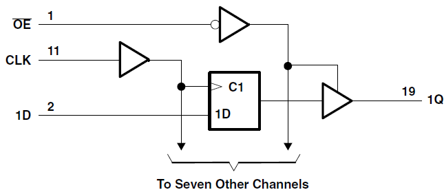
 Logic Diagram
(Positive Logic)