SCLS534D august 2003 – august 2023 SN74LV86A-Q1
PRODUCTION DATA
- 1
- 1Features
- 2Description
- 3Revision History
- 4Pin Configuration and Functions
-
5Specifications
- 5.1 Absolute Maximum Ratings
- 5.2 ESD Ratings
- 5.3 Recommended Operating Conditions
- 5.4 Thermal Information
- 5.5 Electrical Characteristics
- 5.6 Switching Characteristics, VCC = 2.5 V ±0.2 V
- 5.7 Switching Characteristics, VCC = 3.3 V ±0.3 V
- 5.8 Switching Characteristics, VCC = 5 V ±0.5 V
- 5.9 Noise Characteristics
- 5.10 Operating Characteristics
- 6Parameter Measurement Information
- 7Detailed Description
- 8Device and Documentation Support
- 9Mechanical, Packaging, and Orderable Information
Package Options
Refer to the PDF data sheet for device specific package drawings
Mechanical Data (Package|Pins)
- PW|14
Thermal pad, mechanical data (Package|Pins)
- PW|14
Orderable Information
2 Description
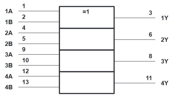
The SN74LV86A-Q1 is a quadruple 2-input exclusive-OR gate designed for 2-V to 5.5-V VCC operation.
Package Information
| PART NUMBER | PACKAGE1 | PACKAGE SIZE 2 |
|---|---|---|
| SN74LV86A-Q1 | PW (TSSOP, 14) | 5.00 mm × 6.4 mm |
(1) For all available packages, see the orderable addendum at the
end of the data sheet.
(2) The package size (length × width)
is a nominal value and includes pins, where applicable.
 Logic
Symbol
Logic
SymbolThis symbol is in accordance with ANSI/IEEE Std 91-1984 and IEC Publication 617-12.