SCLS907A December 2022 – April 2023 SN74LV8T245
PRODUCTION DATA
- 1 Features
- 2 Applications
- 3 Description
- 4 Revision History
- 5 Pin Configuration and Functions
-
6 Specifications
- 6.1 Absolute Maximum Ratings
- 6.2 ESD Ratings
- 6.3 Recommended Operating Conditions
- 6.4 Thermal Information
- 6.5 Electrical Characteristics
- 6.6 Switching Characteristics - 1.8-V VCC
- 6.7 Switching Characteristics - 2.5-V VCC
- 6.8 Switching Characteristics - 3.3-V VCC
- 6.9 Switching Characteristics - 5-V VCC
- 6.10 Noise Characteristics
- 6.11 Typical Characteristics
- 7 Parameter Measurement Information
- 8 Detailed Description
- 9 Application and Implementation
- 10Power Supply Recommendations
- 11Layout
- 12Device and Documentation Support
- 13Mechanical, Packaging, and Orderable Information
Package Options
Mechanical Data (Package|Pins)
Thermal pad, mechanical data (Package|Pins)
- RKS|20
Orderable Information
3 Description
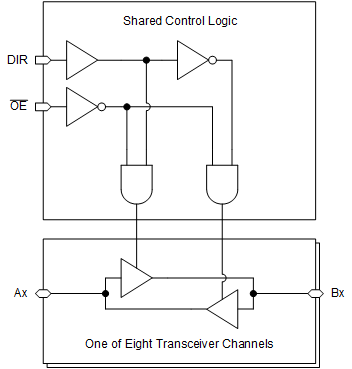
The SN74LV8T245 is an octal bus transceiver with 3-state outputs. All eight channels are controlled by the direction (DIR) pin and output enable (OE) pin. The output level is referenced to the supply voltage (VCC) and supports 1.8-V, 2.5-V, 3.3-V, and 5-V CMOS levels.
The input is designed with a lower threshold circuit to support up translation for lower voltage CMOS inputs (for example, 1.2 V input to 1.8 V output or 1.8 V input to 3.3 V output). Additionally, the 5-V tolerant input pins enable down translation (for example, 3.3 V to 2.5 V output).
| PART NUMBER | PACKAGE | BODY SIZE (NOM) |
|---|---|---|
| SN74LV8T245 | RKS (VQFN, 20) | 4.50 mm × 2.50 mm |
| DGS (VSSOP, 20) | 5.10 mm × 3.00 mm | |
| PW (TSSOP, 20) | 6.50 mm × 4.40 mm |
 Simplified Logic
Diagram (Positive Logic)