SCAS699C August 2003 – June 2014 SN74LVC16244A
PRODUCTION DATA.
- 1 Features
- 2 Applications
- 3 Description
- 4 Simplified Schematic
- 5 Revision History
- 6 Pin Configuration and Functions
-
7 Specifications
- 7.1 Absolute Maximum Ratings
- 7.2 Handling Ratings
- 7.3 Recommended Operating Conditions
- 7.4 Thermal Information
- 7.5 Electrical Characteristics—DC Limit Changes
- 7.6 Switching Characteristics, -40°C to 85°C
- 7.7 Switching Characteristics, -40°C to 125°C
- 7.8 Operating Characteristics
- 7.9 Typical Characteristics
- 8 Parameter Measurement Information
- 9 Detailed Description
- 10Application and Implementation
- 11Power Supply Recommendations
- 12Layout
- 13Device and Documentation Support
- 14Mechanical, Packaging, and Orderable Information
Package Options
Refer to the PDF data sheet for device specific package drawings
Mechanical Data (Package|Pins)
- DGG|48
- DL|48
- DGV|48
Thermal pad, mechanical data (Package|Pins)
Orderable Information
6 Pin Configuration and Functions
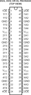
Pin Functions
| PIN | I/O | DESCRIPTION | |
|---|---|---|---|
| NO. | NAME | ||
| 1 | 1OE | I | Output enable 1 |
| 2 | 1Y1 | O | 1Y1 Output |
| 3 | 1Y2 | O | 1Y2 Output |
| 4 | GND | — | Ground pin |
| 5 | 1Y3 | O | 1Y3 Output |
| 6 | 1Y4 | O | 1Y4 Output |
| 7 | VCC | — | Power pin |
| 8 | 2Y1 | O | 2Y1 Output |
| 9 | 2Y2 | O | 2Y2 Output |
| 10 | GND | — | Ground pin |
| 11 | 2Y3 | O | 2Y3 Output |
| 12 | 2Y4 | O | 2Y4 Output |
| 13 | 3Y1 | O | 3Y1 Output |
| 14 | 3Y2 | O | 3Y2 Output |
| 15 | GND | — | Ground pin |
| 16 | 3Y3 | O | 3Y3 Output |
| 17 | 3Y4 | O | 3Y4 Output |
| 18 | VCC | — | Power pin |
| 19 | 4Y1 | O | 4Y1 Output |
| 20 | 4Y2 | O | 4Y2 Output |
| 21 | GND | — | Ground pin |
| 22 | 4Y3 | O | 4Y3 Output |
| 23 | 4Y4 | O | 4Y4 Output |
| 24 | 4OE | I | Output enable 4 |
| 25 | 3OE | I | Output enable 3 |
| 26 | 4A4 | I | 4A4 Input |
| 27 | 4A3 | I | 4A3 Input |
| 28 | GND | — | Ground pin |
| 29 | 4A2 | I | 4A2 Input |
| 30 | 4A1 | I | 4A1 Input |
| 31 | VCC | — | Power pin |
| 32 | 3A4 | I | 3A4 Input |
| 33 | 3A3 | I | 3A3 Input |
| 34 | GND | — | Ground pin |
| 35 | 3A2 | I | 3A2 Input |
| 36 | 3A1 | I | 3A1 Input |
| 37 | 2A4 | I | 2A4 Input |
| 38 | 2A3 | I | 2A3 Input |
| 39 | GND | — | Ground pin |
| 40 | 2A2 | I | 2A2 Input |
| 41 | 2A1 | I | 2A1 Input |
| 42 | VCC | — | Power pin |
| 43 | 1A4 | I | 1A4 Input |
| 44 | 1A3 | I | 1A3 Input |
| 45 | GND | — | Ground pin |
| 46 | 1A2 | I | 1A2 Input |
| 47 | 1A1 | I | 1A1 Input |
| 48 | 2OE | I | Output enable 2 |
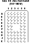
Table 1. Pin Assignments(1) (56-Ball GQL or ZQL Package)
| 1 | 2 | 3 | 4 | 5 | 6 | |
|---|---|---|---|---|---|---|
| A | 1OE | NC | NC | NC | NC | 2OE |
| B | 1Y2 | 1Y1 | GND | GND | 1A1 | 1A2 |
| C | 1Y4 | 1Y3 | VCC | VCC | 1A3 | 1A4 |
| D | 2Y2 | 2Y1 | GND | GND | 2A1 | 2A2 |
| E | 2Y4 | 2Y3 | 2A3 | 2A4 | ||
| F | 3Y1 | 3Y2 | 3A2 | 3A1 | ||
| G | 3Y3 | 3Y4 | GND | GND | 3A4 | 3A3 |
| H | 4Y1 | 4Y2 | VCC | VCC | 4A2 | 4A1 |
| J | 4Y3 | 4Y4 | GND | GND | 4A4 | 4A3 |
| K | 4OE | NC | NC | NC | NC | 3OE |
(1) NC – No internal connection
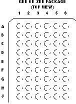
Table 2. Pin Assignments(1) (54-Ball GRD or ZRD Package)
| 1 | 2 | 3 | 4 | 5 | 6 | |
|---|---|---|---|---|---|---|
| A | 1Y1 | NC | 1OE | 2OE | NC | 1A1 |
| B | 1Y3 | 1Y2 | NC | NC | 1A2 | 1A3 |
| C | 2Y1 | 1Y4 | VCC | VCC | 1A4 | 2A1 |
| D | 2Y3 | 2Y2 | GND | GND | 2A2 | 2A3 |
| E | 3Y1 | 2Y4 | GND | GND | 2A4 | 3A1 |
| F | 3Y3 | 3Y2 | GND | GND | 3A2 | 3A3 |
| G | 4Y1 | 3Y4 | VCC | VCC | 3A4 | 4A1 |
| H | 4Y3 | 4Y2 | NC | NC | 4A2 | 4A3 |
| J | 4Y4 | NC | 4OE | 3OE | NC | 4A4 |
(1) NC – No internal connection