SCAS755B December 2003 – June 2014 SN74LVC16373A
PRODUCTION DATA.
- 1 Features
- 2 Applications
- 3 Description
- 4 Simplified Schematic
- 5 Revision History
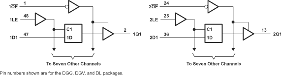
- 6 Pin Configuration and Functions
- 7 Specifications
- 8 Parameter Measurement Information
- 9 Detailed Description
- 10Application and Implementation
- 11Power Supply Recommendations
- 12Layout
- 13Device and Documentation Support
- 14Mechanical, Packaging, and Orderable Information
Package Options
Refer to the PDF data sheet for device specific package drawings
Mechanical Data (Package|Pins)
- DGG|48
- DL|48
- DGV|48
Thermal pad, mechanical data (Package|Pins)
Orderable Information
1 Features
- Member of the Texas Instruments
Widebus™ Family - Operates From 1.65 V to 3.6 V
- Inputs Accept Voltages to 5.5 V
- Max tpd of 4.2 ns at 3.3 V
- Typical VOLP (Output Ground Bounce)
<0.8 V at VCC = 3.3 V, TA = 25°C - Typical VOHV (Output VOH Undershoot)
>2 V at VCC = 3.3 V, TA = 25°C - Ioff Supports Live-Insertion, Partial-Power-Down Mode, and Back-Drive Protection
- Supports Mixed-Mode Signal Operation (5-V Input and Output Voltages With 3.3-V VCC)
- Latch-Up Performance Exceeds 100 mA Per
JESD 78, Class II - ESD Protection Exceeds JESD 22
- 2000-V Human-Body Model (A114-A)
- 1000-V Charged-Device Model (C101)
2 Applications
3 Description
The SN74LVC16373A device is a 16-bit transparent D-type latch which is designed for 1.65-V to 3.6-V VCC operation.
Device Information(1)
| PART NUMBER | PACKAGE | BODY SIZE (NOM) |
|---|---|---|
| SN74LVC16373A | TSSOP (48) | 12.50 mm × 6.10 mm |
| TVSOP (48) | 9.70 mm × 4.40 mm | |
| SSOP (48) | 15.80 mm × 7.49 mm | |
| BGA MICROSTAR JUNIOR (56) | 7.00 mm × 4.50 mm | |
| BGA MICROSTAR JUNIOR (54) | 8.00 mm × 5.50 mm |
- For all available packages, see the orderable addendum at the end of the data sheet.
4 Simplified Schematic