SCES213X April 1999 – April 2014 SN74LVC1G02
PRODUCTION DATA.
- 1 Features
- 2 Applications
- 3 Description
- 4 Revision History
- 5 Pin Configuration and Functions
-
6 Specifications
- 6.1 Absolute Maximum Ratings
- 6.2 Handling Ratings
- 6.3 Recommended Operating Conditions
- 6.4 Thermal Information
- 6.5 Electrical Characteristics
- 6.6 Switching Characteristics, CL = 15 pF
- 6.7 Switching Characteristics, -40°C to 85°C
- 6.8 Switching Characteristics, -40°C to 125°C
- 6.9 Operating Characteristics
- 6.10 Typical Characteristics
- 7 Parameter Measurement Information
- 8 Detailed Description
- 9 Application and Implementation
- 10Power Supply Recommendations
- 11Layout
- 12Device and Documentation Support
- 13Mechanical, Packaging, and Orderable Information
9 Application and Implementation
9.1 Application Information
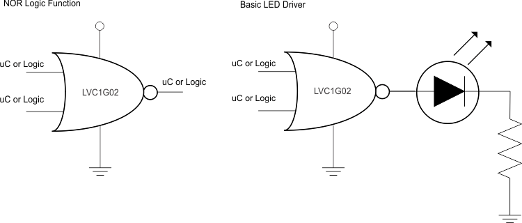
The SN74LVC1G02 is a high drive CMOS device that can be used for implement NOR logic with a high output drive, such as an LED application. It can produce 24-mA of drive current at 3.3 V making it Ideal for driving multiple outputs and good for high speed applications up to 100 Mhz. The inputs are 5.5-V tolerant allowing translation down to VCC.
9.2 Typical Application
9.2.1 Design Requirements
This device uses CMOS technology and has balanced output drive. Care should be taken to avoid bus contention because it can drive currents that would exceed maximum limits. The high drive will also create fast edges into light loads, so routing and load conditions should be considered to prevent ringing.
9.2.2 Detailed Design Procedure
- Recommended Input Conditions:
- Rise time and fall time specs. See (Δt/ΔV) in the Recommended Operating Conditions table.
- Specified high and low levels. See (VIH and VIL) in the Recommended Operating Conditions table.
- Inputs are overvoltage tolerant allowing them to go as high as (VI max) in the Recommended Operating Conditions table at any valid VCC.
- Recommend Output Conditions:
- Load currents should not exceed (IO max) per output and should not exceed total current (continuous current through VCC or GND) for the part. These limits are located in the Absolute Maximum Ratings table.
- Outputs should not be pulled above VCC.
9.2.3 Application Curves
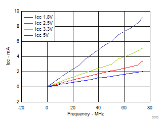 Figure 5. ICC vs Frequency