SCES224R April 1999 – January 2015 SN74LVC1G126
PRODUCTION DATA.
- 1 Applications
- 2 Simplified Schematic
- 3 Revision History
- 4 Pin Configuration and Functions
- 5 Specifications
- 6 Parameter Measurement Information
- 7 Detailed Description
- 8 Application and Implementation
- 9 Power Supply Recommendations
- 10Layout
- 11Device and Documentation Support
- 12Mechanical, Packaging, and Orderable Information
Package Options
Refer to the PDF data sheet for device specific package drawings
Mechanical Data (Package|Pins)
- DBV|5
- DSF|6
- DCK|5
- DRL|5
- DRY|6
- YZP|5
Thermal pad, mechanical data (Package|Pins)
- DRY|6
Orderable Information
7 Detailed Description
7.1 Overview
The SN74LVC1G126 device contains a dual buffer gate with output enable control and performs the Boolean function Y = A.
This device is fully specified for partial-power-down applications using Ioff. The Ioff circuitry disables the outputs, preventing damaging current backflow through the device when it is powered down.
To ensure the high-impedance state during power up or power down, OE should be tied to GND through a pull-down resistor; the minimum value of the resistor is determined by the current-sourcing capability of the driver.
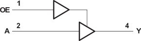
7.2 Functional Block Diagram
7.3 Feature Description
- 1.65 V to 5.5 V operating voltage range
- Allows down voltage translation
- 5 V to 3.3 V
- 5 V or 3.3 V to 1.8 V
- Inputs accept voltages to 5.5 V
- 5.5-V tolerance on input pin when VCC = 0 V
- Ioff feature
- Allows voltage on the inputs and outputs when VCC is 0 V
- Able to reduce leakage when VCC is 0 V
7.4 Device Functional Modes
Table 1. Function Table
| INPUTS | OUTPUT Y |
|
|---|---|---|
| OE | A | |
| H | H | H |
| H | L | L |
| L | X | Z |