SCES224R April   1999  – January 2015 SN74LVC1G126

PRODUCTION DATA.  

  1. Applications
  2. Simplified Schematic
  3. Revision History
  4. Pin Configuration and Functions
  5. Specifications
    1. 5.1 Absolute Maximum Ratings
    2. 5.2 ESD Ratings
    3. 5.3 Thermal Information
    4. 5.4 Switching Characteristics, -40°C to 125°C
    5. 5.5 Operating Characteristics
    6. 5.6 Typical Characteristics
  6. Parameter Measurement Information
  7. Detailed Description
    1. 7.1 Overview
    2. 7.2 Functional Block Diagram
    3. 7.3 Feature Description
    4. 7.4 Device Functional Modes
  8. Application and Implementation
    1. 8.1 Application Information
    2. 8.2 Typical Application
      1. 8.2.1 Design Requirements
      2. 8.2.2 Detailed Design Procedure
      3. 8.2.3 Application Curves
  9. Power Supply Recommendations
  10. 10Layout
    1. 10.1 Layout Guidelines
    2. 10.2 Layout Example
  11. 11Device and Documentation Support
    1. 11.1 Glossary
  12. 12Mechanical, Packaging, and Orderable Information
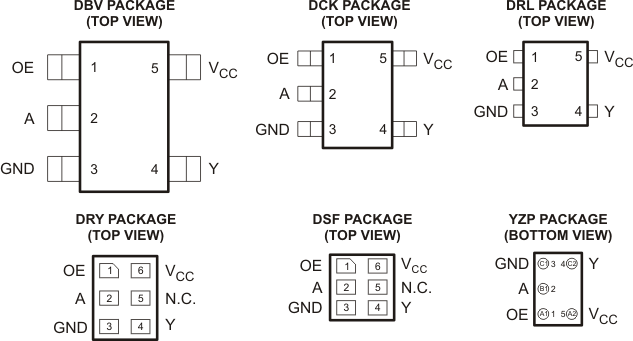
Package Options

Refer to the PDF data sheet for device specific package drawings

Mechanical Data (Package|Pins)
  • DBV|5
  • DSF|6
  • DCK|5
  • DRL|5
  • DRY|6
  • YZP|5
Thermal pad, mechanical data (Package|Pins)
Orderable Information

4 Pin Configuration and Functions

po2_ces224.gif
See mechanical drawings for dimensions.

Pin Functions

PIN TYPE DESCRIPTION
NAME SN74LVC1G126
DBV, DCK, DRL, YZP DRY, DSF
A 2 2 I A Input
GND 3 3 Ground Pin
NC 5 Do not connect
OE 1 1 I OE Enable/Input
VCC 5 6 Power Pin
Y 4 4 O Y Output