SCES560G March 2004 – June 2015 SN74LVC1G175
PRODUCTION DATA.
- 1 Features
- 2 Applications
- 3 Description
- 4 Revision History
- 5 Pin Configuration and Functions
-
6 Specifications
- 6.1 Absolute Maximum Ratings
- 6.2 ESD Ratings
- 6.3 Recommended Operating Conditions
- 6.4 Thermal Information
- 6.5 Electrical Characteristics
- 6.6 Timing Requirements, -40°C to 85°C
- 6.7 Timing Requirements, -40°C to 125°C
- 6.8 Switching Characteristics, -40°C to 85°C
- 6.9 Switching Characteristics, -40°C to 85°C
- 6.10 Switching Characteristics, -40°C to 125°C
- 6.11 Operating Characteristics
- 6.12 Typical Characteristics
- 7 Parameter Measurement Information
- 8 Detailed Description
- 9 Application and Implementation
- 10Power Supply Recommendations
- 11Layout
- 12Device and Documentation Support
- 13Mechanical, Packaging, and Orderable Information
Package Options
Mechanical Data (Package|Pins)
Thermal pad, mechanical data (Package|Pins)
- DRY|6
Orderable Information
1 Features
- Available in the Texas Instruments
NanoFree™ Package - Supports 5-V VCC Operation
- Inputs Accept Voltages to 5.5 V
- Supports Down Translation to VCC
- Max tpd of 4.3 ns at 3.3 V
- Low Power Consumption, 10-µA Max ICC
- ±24-mA Output Drive at 3.3 V
- Ioff Supports Live Insertion, Partial-Power-Down Mode, and Back-Drive Protection
- Latch-Up Performance Exceeds 100 mA Per JESD 78, Class II
- ESD Protection Exceeds JESD 22
- 2000-V Human-Body Model (A114-A)
- 200-V Machine Model (A115-A)
- 1000-V Charged-Device Model (C101)
2 Applications
- TV/Set Top Box/Audio
- EPOS (Electronic Point-of-Sale)
- Motor Drives
- PC/Notebook
- Servers
- Factory Automation and Control
- Tablets
- Medical Healthcare and Fitness
- Smart Grid
- Telecom Infrastructure
- Enterprise Switching
- Projectors
- Storage
3 Description
This single D-type flip-flop is designed for 1.65-V to 5.5-V VCC operation.
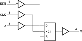
The SN74LVC1G175 device has an asynchronous clear (CLR) input. When CLR is high, data from the input pin (D) is transferred to the output pin (Q) on the clock's (CLK) rising edge. When CLR is low, Q is forced into the low state, regardless of the clock edge or data on D.
NanoFree™ package technology is a major breakthrough in IC packaging concepts, using the die as the package.
This device is fully specified for partial-power-down applications using Ioff. The Ioff circuitry disables the outputs, preventing damaging current backflow through the device when it is powered down.
Device Information(1)
| PART NUMBER | PACKAGE | BODY SIZE (NOM) |
|---|---|---|
| SN74LVC1G175DBV | SOT-23 (6) | 2.90 mm × 1.60 mm |
| SN74LVC1G175DCK | SC70 (6) | 2.00 mm × 1.25 mm |
| SN74LVC1G175DRY | SON (6) | 1.45 mm × 1.00 mm |
| SN74LVC1G175YZP | DSBGA (6) | 1.41 mm × 0.91 mm |
- For all available packages, see the orderable addendum at the end of the data sheet.
Logic Diagram (Positive Logic)
