SCES560G March 2004 – June 2015 SN74LVC1G175
PRODUCTION DATA.
- 1 Features
- 2 Applications
- 3 Description
- 4 Revision History
- 5 Pin Configuration and Functions
-
6 Specifications
- 6.1 Absolute Maximum Ratings
- 6.2 ESD Ratings
- 6.3 Recommended Operating Conditions
- 6.4 Thermal Information
- 6.5 Electrical Characteristics
- 6.6 Timing Requirements, -40°C to 85°C
- 6.7 Timing Requirements, -40°C to 125°C
- 6.8 Switching Characteristics, -40°C to 85°C
- 6.9 Switching Characteristics, -40°C to 85°C
- 6.10 Switching Characteristics, -40°C to 125°C
- 6.11 Operating Characteristics
- 6.12 Typical Characteristics
- 7 Parameter Measurement Information
- 8 Detailed Description
- 9 Application and Implementation
- 10Power Supply Recommendations
- 11Layout
- 12Device and Documentation Support
- 13Mechanical, Packaging, and Orderable Information
Package Options
Mechanical Data (Package|Pins)
Thermal pad, mechanical data (Package|Pins)
- DRY|6
Orderable Information
9 Application and Implementation
NOTE
Information in the following applications sections is not part of the TI component specification, and TI does not warrant its accuracy or completeness. TI’s customers are responsible for determining suitability of components for their purposes. Customers should validate and test their design implementation to confirm system functionality.
9.1 Application Information
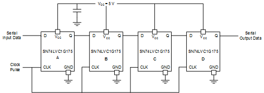
Multiple SN74LVC1G175 devices can be used in tandem to create a shift register of arbitrary length. In this example, we use four SN74LVC1G175 devices to form a 4-bit serial shift register. By connecting all CLK inputs to a common clock pulse and tying each output of one device to the next, we can store and load 4-bit values on demand. We demonstrate loading the 4 bit value 1101 into memory by setting Serial Input Data to each desired memory bit, and by sending a clock pulse for each bit, we sequentially move all stored bits from left to right
(A → B → C → D)
9.2 Typical Application
 Figure 4. 4-Bit Serial Shift Register
Table 2. Stored Data Values
| Serial Input Data | Stored A | Stored B | Stored C | Stored D |
|---|---|---|---|---|
| 1 | 0 | 0 | 0 | 0 |
| 0 | 1 | 0 | 0 | 0 |
| 1 | 0 | 1 | 0 | 0 |
| 1 | 1 | 0 | 1 | 0 |
| 0 | 1 | 1 | 0 | 1 |
9.2.1 Design Requirements
The SN74LVC1G175 device uses CMOS technology and has balanced output drive. Care must be taken to avoid bus contention because it can drive currents that would exceed maximum limits.
The SN74LVC1G175 allows storing digital signals with a digital control signal. All input signals should remain as close as possible to either 0 V or VCC for optimal operation.
9.2.2 Detailed Design Procedure
- Recommended input conditions:
- For rise time and fall time specifications, see Δt/Δv in the table.
- For specified high and low levels, see VIH and VIL in the table.
- Inputs and outputs are overvoltage tolerant and can therefore go as high as 5.5 V at any valid VCC.
- Recommended output conditions:
- Load currents should not exceed ±50 mA.
- Frequency selection criterion:
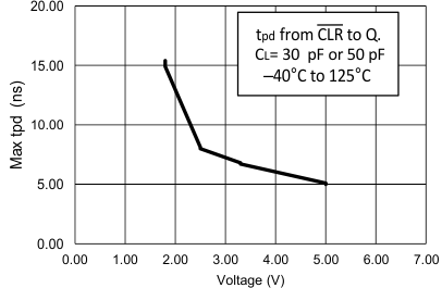
- The effects of frequency upon the output current should be studied in Figure 5.
- Added trace resistance and capacitance can reduce maximum frequency capability; follow the layout practices listed in the Layout section.
9.2.3 Application Curve
 Figure 5. Max tpd vs Voltage of LVC Family