SCES463H June 2003 – December 2021 SN74LVC1G3157-Q1
PRODUCTION DATA
- 1 Features
- 2 Applications
- 3 Description
- 4 Revision History
- 5 Pin Configuration and Functions
- 6 Specifications
- 7 Parameter Measurement Information
- 8 Detailed Description
- 9 Application and Implementation
- 10Power Supply Recommendations
- 11Layout
- 12Device and Documentation Support
- 13Mechanical, Packaging, and Orderable Information
Package Options
Refer to the PDF data sheet for device specific package drawings
Mechanical Data (Package|Pins)
- DBV|6
- DCK|6
Thermal pad, mechanical data (Package|Pins)
Orderable Information
9.2.2 Detailed Design Procedure
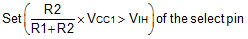
Using this circuit idea, a system designer can ensure a component or subsystem power has ramped up before allowing signals to be applied to its input. This is useful for integrated circuits that do not have overvoltage tolerant inputs. The basic idea uses a resistor divider on the VCC1 power rail, which is ramping up. The RC time constant of the resistor divider further delays the voltage ramp on the select pin of the SPDT bus switch. By carefully selecting values for R1, R2 and C, it is possible to ensure that VCC1 will reach its nominal value before the path from A to B2 is established, thus preventing a signal being present on an I/O before the device/system is powered up. To ensure the minimum desired delay is achieved, the designer should use Equation 1 to calculate the time required from a transition from ground (0 V) to half the supply voltage (VCC1/2).
Choose Rs and C to achieve the desired delay.
When Vs goes high, the signal will be passed.