SCES874 March 2017 SN74LVC1G79-Q1
PRODUCTION DATA.
- 1 Features
- 2 Applications
- 3 Description
- 4 Revision History
- 5 Pin Configuration and Functions
-
6 Specifications
- 6.1 Absolute Maximum Ratings
- 6.2 ESD Ratings
- 6.3 Recommended Operating Conditions
- 6.4 Thermal Information
- 6.5 Electrical Characteristics
- 6.6 Timing Requirements
- 6.7 Timing Requirements
- 6.8 Switching Characteristics: CL = 15 pF, TA = -40°C to +85°C
- 6.9 Switching Characteristics: CL = 30 or 50 pF, TA = -40°C to +85°C
- 6.10 Switching Characteristics: CL = 30 pF or 50 pF, TA = -40°C to +125°C
- 6.11 Operating Characteristics
- 6.12 Typical Characteristics
- 7 Parameter Measurement Information
- 8 Detailed Description
- 9 Application and Implementation
- 10Power Supply Recommendations
- 11Layout
- 12Device and Documentation Support
- 13Mechanical, Packaging, and Orderable Information
Package Options
Mechanical Data (Package|Pins)
- DCK|5
Thermal pad, mechanical data (Package|Pins)
Orderable Information
8 Detailed Description
8.1 Overview
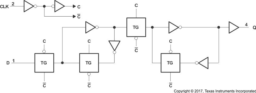
The SN74LVC1G79-Q1 is a single positive-edge-triggered D-type flip-flop and is AEC-Q100 qualified for automotive applications. Data at the input (D) is transferred to the output (Q) on the positive-going edge of the clock pulse when the setup time requirement is met. Because the clock triggering occurs at a voltage level, it is not directly related to the rise time of the clock pulse. This allows for data at the input to be changed without affecting the level at the output, following the hold-time interval.
8.2 Functional Block Diagram
 Figure 5. Logic Diagram (Positive Logic)
8.3 Feature Description
8.3.1 Balanced High-Drive CMOS Push-Pull Outputs
A balanced output allows the device to sink and source similar currents. The high drive capability of this device creates fast edges into light loads so routing and load conditions should be considered to prevent ringing. Additionally, the outputs of this device are capable of driving larger currents than the device can sustain without being damaged. It is important for the power output of the device to be limited to avoid thermal runaway and damage due to over-current. The electrical and thermal limits defined the in the Absolute Maximum Ratings must be followed at all times.
8.3.2 Standard CMOS Inputs
Standard CMOS inputs are high impedance and are typically modeled as a resistor in parallel with the input capacitance given in the Electrical Characteristics. The worst case resistance is calculated with the maximum input voltage, given in the Recommended Operating Conditions, and the maximum input leakage current, given in the Electrical Characteristics, using ohm's law (R = V ÷ I).
Signals applied to the inputs need to have fast edge rates, as defined by Δt/Δv in Recommended Operating Conditions to avoid excessive currents and oscillations. If tolerance to a slow or noisy input signal is required, a device with a Schmitt-trigger input should be utilized to condition the input signal prior to the standard CMOS input.
8.3.3 Clamp Diodes
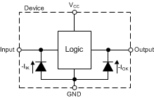
The inputs and outputs to this device have negative clamping diodes.
CAUTION
Voltages beyond the values specified in the Absolute Maximum Ratings table can cause damage to the device. The input negative-voltage and output voltage ratings may be exceeded if the input and output clamp-current ratings are observed.
 Figure 6. Electrical Placement of Clamping Diodes for Each Input and Output
8.3.4 Partial Power Down (Ioff)
The inputs and outputs for this device enter a high impedance state when the supply voltage is 0 V. The maximum leakage into or out of any input or output pin on the device is specified by Ioff in the Electrical Characteristics.
8.3.5 Over-Voltage Tolerant Inputs
Input signals to this device can be driven above the supply voltage so long as they remain below the maximum input voltage value specified in the Absolute Maximum Ratings.
8.4 Device Functional Modes
Table 1 shows the functional modes of SN74LVC1G79-Q1.
Table 1. Function Table
| INPUTS | OUTPUT Y |
|
|---|---|---|
| CLK | D | |
| ↑ | H | H |
| ↑ | L | L |
| L | X | Q0 |