SCES193N April 1999 – January 2015 SN74LVC2G00
PRODUCTION DATA.
- 1 Features
- 2 Applications
- 3 Description
- 4 Simplified Schematic
- 5 Revision History
- 6 Pin Configuration and Functions
- 7 Specifications
- 8 Parameter Measurement Information
- 9 Detailed Description
- 10Application and Implementation
- 11Power Supply Recommendations
- 12Layout
- 13Device and Documentation Support
- 14Mechanical, Packaging, and Orderable Information
Package Options
Refer to the PDF data sheet for device specific package drawings
Mechanical Data (Package|Pins)
- DCU|8
- YZP|8
- DCT|8
Thermal pad, mechanical data (Package|Pins)
Orderable Information
6 Pin Configuration and Functions
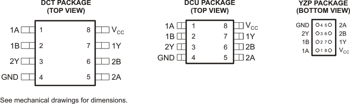
Pin Functions
| PIN | TYPE | DESCRIPTION | |
|---|---|---|---|
| NAME | DCT, DCU, YZP | ||
| 1A | 1 | I | A input for gate 1 |
| 1B | 2 | I | B input for gate 1 |
| 2Y | 3 | O | Output for gate 2 |
| GND | 4 | — | Ground |
| 2A | 5 | I | A input for gate 2 |
| 2B | 6 | I | B input for gate 2 |
| 1Y | 7 | O | Output for gate 1 |
| VCC | 8 | I | Power input. |