SCES381N January 2002 – January 2015 SN74LVC2G17 , SN74LVC2G17
PRODUCTION DATA.
- 1 Features
- 2 Applications
- 3 Simplified Schematic
- 4 Revision History
- 5 Pin Configuration and Functions
- 6 Specifications
- 7 Parameter Measurement Information
- 8 Detailed Description
- 9 Application and Implementation
- 10Power Supply Recommendations
- 11Layout
- 12Device and Documentation Support
- 13Mechanical, Packaging, and Orderable Information
Package Options
Mechanical Data (Package|Pins)
Thermal pad, mechanical data (Package|Pins)
- DRY|6
Orderable Information
1 Features
- Schmitt-Trigger inputs provide hysteresis
- Available in the Texas Instruments
NanoFree™ Package - Supports 5-V VCC Operation
- Inputs Accept Voltages to 5.5 V
- Max tpd of 5.4 ns at 3.3 V
- Low Power Consumption, 10-μA Max ICC
- ±24-mA Output Drive at 3.3 V
- Typical VOLP (Output Ground Bounce)
< 0.8 V at VCC = 3.3 V, TA = 25°C - Typical VOHV (Output VOH Undershoot)
> 2 V at VCC = 3.3 V, TA = 25°C - Ioff Supports Live Insertion, Partial-Power-Down Mode Operation and Back-Drive Protection
- Latch-Up Performance Exceeds 100 mA
Per JESD 78, Class II - ESD Protection Exceeds JESD 22
- 2000-V Human-Body Model
- 1000-V Charged-Device Model
2 Applications
- AV Receivers
- Audio Docks: Portable
- Blu-ray Players and Home Theater
- MP3 Players/Recorders
- Personal Digital Assistants (PDAs)
- Power: Telecom/Server AC/DC Supply: Single Controller: Analog and Digital
- Solid State Drives (SSDs): Client and Enterprise
- TVs: LCD/Digital and High-Definition (HDTVs)
- Tablets: Enterprise
- Video Analytics: Server
- Wireless Headsets, Keyboards, and Mice
Description
This dual Schmitt-Trigger buffer is designed for 1.65-V to 5.5-V VCC operation.
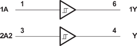
The SN74LVC2G17 device contains two buffers and performs the Boolean function Y = A. The device functions as two independent buffers, but because of Schmitt action, it may have different input threshold levels for positive-going (VT+) and negative-going (VT–) signals.
NanoFree™ package technology is a major breakthrough in IC packaging concepts, using the die as the package.
This device is fully specified for partial-power-down applications using Ioff. The Ioff circuitry disables the outputs, preventing damaging current backflow through the device when it is powered down.
Device Information(1)
| PART NUMBER | PACKAGE (PIN) | BODY SIZE |
|---|---|---|
| SN74LVC2G17 | SOT-23 (6) | 2.90 mm × 1.60 mm |
| SC70 (6) | 2.00 mm × 1.25 mm | |
| SON (6) | 1.45 mm × 1.00 mm | |
| SON (6) | 1.00 mm × 1.00 mm | |
| DSBGA (6) | 1.41 mm × 0.91 mm |
- For all available packages, see the orderable addendum at the end of the data sheet.
3 Simplified Schematic