SCAS286S January 1993 – March 2024 SN54LVC32A , SN74LVC32A
PRODUCTION DATA
- 1
- 1 Features
- 2 Applications
- 3 Description
- 4 Pin Configuration and Functions
-
5 Specifications
- 5.1 Absolute Maximum Ratings
- 5.2 ESD Ratings
- 5.3 Recommended Operating Conditions, SN54LVC32A
- 5.4 Recommended Operating Conditions, SN74LVC32A
- 5.5 Thermal Information
- 5.6 Electrical Characteristics, SN54LVC32A
- 5.7 Electrical Characteristics, SN74LVC32A
- 5.8 Switching Characteristics, SN54LVC32A
- 5.9 Switching Characteristics, SN74LVC32A
- 5.10 Operating Characteristics
- 5.11 Typical Characteristics
- 6 Parameter Measurement Information
- 7 Detailed Description
- Application and Implementation
- 8 Device and Documentation Support
- 9 Glossary
- 10Revision History
- 11Mechanical, Packaging, and Orderable Information
Package Options
Refer to the PDF data sheet for device specific package drawings
Mechanical Data (Package|Pins)
- D|14
- RGY|14
- DB|14
- PW|14
- BQA|14
- NS|14
Thermal pad, mechanical data (Package|Pins)
Orderable Information
3 Description
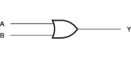
The SN54LVC32A quadruple 2-input positive-OR gate is designed for 2.7V to 3.6V VCC operation, and the SN74LVC32A quadruple 2-input positive-OR gate is designed for 1.65V to 3.6V VCC operation.
The SNx4LVC32A devices perform the Boolean function 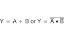 in positive
logic.
in positive
logic.
Inputs can be driven from either 3.3V or 5V devices. This feature allows the use of these devices as translators in a mixed 3.3V/5V system environment.
Device Information
| PART NUMBER | PACKAGE(1) | PACKAGE SIZE(2) | BODY SIZE(3) |
|---|---|---|---|
| SNx4LVC32A | BQA (WQFN, 14) | 3mm × 2.5mm | 3mm × 2.5mm |
| D (SOIC, 14) | 8.65mm × 6mm | 8.65mm × 3.91mm | |
| DB (SSOP, 14) | 6.2mm × 7.8mm | 6.20mm × 5.30mm | |
| NS (SOP, 14) | 10.2mm × 7.8mm | 10.30mm × 5.30mm | |
| PW (TSSOP, 14) | 5mm × 6.4mm | 5.00mm × 4.40mm | |
| RGY (VQFN, 14) | 3.50mm × 3.50mm | 3.50mm × 3.50mm | |
| FK (LCCC, 20) | 8.9mm x 8.9mm | 8.9mm x 8.9mm | |
| J (CDIP, 14) | 19.55mm x 7.9mm | 19.55 mm x 6.7mm | |
| W (CFP, 14) | 9.21mm x 9mm | 9.21mm x 6.28mm |
(1) For more information, see Section
11.
(2) The package size (length × width)
is a nominal value and includes pins, where applicable.
(3) The body size (length × width) is
a nominal value and does not include pins.
Simplified Schematic