SCAS306K March 1993 – December 2014 SN74LVC827A
PRODUCTION DATA.
- 1 Features
- 2 Applications
- 3 Description/Ordering Information
- 4 Revision History
- 5 Pin Configuration and Functions
- 6 Specifications
- 7 Parameter Measurement Information
- 8 Detailed Description
- 9 Application and Implementation
- 10Power Supply Recommendations
- 11Layout
- 12Device and Documentation Support
- 13Mechanical, Packaging, and Orderable Information
Package Options
Refer to the PDF data sheet for device specific package drawings
Mechanical Data (Package|Pins)
- DGV|24
- DB|24
- DW|24
- PW|24
Thermal pad, mechanical data (Package|Pins)
- DW|24
Orderable Information
8 Detailed Description
8.1 Overview
This 10-bit buffer/bus driver is designed for 1.65-V to 3.6-V VCC operation.
The SN74LVC827A provides a high-performance bus interface for wide data paths or buses carrying parity.
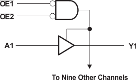
The 3-state control gate is a 2-input AND gate with active-low inputs so that, if either output-enable (OE1 or OE2) input is high, all ten outputs are in the high-impedance state. The SN74LVC827A provides true data at its outputs.
Inputs can be driven from either 3.3-V or 5-V devices. This feature allows the use of this device as a translator in a mixed 3.3-V/5-V system environment.
To ensure the high-impedance state during power up or power down, OE should be tied to VCC through a pullup resistor; the minimum value of the resistor is determined by the current-sinking capability of the driver.
This device is fully specified for partial-power-down applications using Ioff. The Ioff circuitry disables the outputs, preventing damaging current backflow through the device when it is powered down.
8.2 Functional Block Diagram
8.3 Feature Description
- Wide operating voltage range
- Operates from 1.65 V to 3.6 V
- Allows down voltage translation
- Inputs accept voltages to 5.5 V
- Ioff feature
- Allows voltages on the inputs and outputs when VCC is 0 V
8.4 Device Functional Modes
Table 1. Function Table
| INPUTS | OUTPUT Y |
||
|---|---|---|---|
| OE1 | OE2 | A | |
| L | L | L | L |
| L | L | H | H |
| H | X | X | Z |
| X | H | X | Z |