SCAS306K March 1993 – December 2014 SN74LVC827A
PRODUCTION DATA.
- 1 Features
- 2 Applications
- 3 Description/Ordering Information
- 4 Revision History
- 5 Pin Configuration and Functions
- 6 Specifications
- 7 Parameter Measurement Information
- 8 Detailed Description
- 9 Application and Implementation
- 10Power Supply Recommendations
- 11Layout
- 12Device and Documentation Support
- 13Mechanical, Packaging, and Orderable Information
Package Options
Refer to the PDF data sheet for device specific package drawings
Mechanical Data (Package|Pins)
- DGV|24
- DB|24
- DW|24
- PW|24
Thermal pad, mechanical data (Package|Pins)
- DW|24
Orderable Information
5 Pin Configuration and Functions
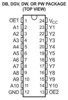
Pin Functions
| PIN | TYPE | DESCRIPTION | |
|---|---|---|---|
| NO. | NAME | ||
| 1 | OE1 | I | Output Enable 1 |
| 2 | A1 | I | A1 Input |
| 3 | A2 | I | A2 Input |
| 4 | A3 | I | A3 Input |
| 5 | A4 | I | A4 Input |
| 6 | A5 | I | A5 Input |
| 7 | A6 | I | A6 Input |
| 8 | A7 | I | A7 Input |
| 9 | A8 | I | A8 Input |
| 10 | A9 | I | A9 Input |
| 11 | A10 | I | A10 Input |
| 12 | GND | — | Ground Pin |
| 13 | OE2 | I | Output Enable 2 |
| 14 | Y10 | O | Y10 Output |
| 15 | Y9 | O | Y9 Output |
| 16 | Y8 | O | Y8 Output |
| 17 | Y7 | O | Y7 Output |
| 18 | Y6 | O | Y6 Output |
| 19 | Y5 | O | Y5 Output |
| 20 | Y4 | O | Y4 Output |
| 21 | Y3 | O | Y3 Output |
| 22 | Y2 | O | Y2 Output |
| 23 | Y1 | O | Y1 Output |
| 24 | VCC | — | Power Pin |