SCES770A December 2008 – March 2017 SN74LVC8T245-EP
PRODUCTION DATA.
- 1 Features
- 2 Applications
- 3 Description
- 4 Revision History
- 5 Description (continued)
- 6 Pin Configuration and Functions
-
7 Specifications
- 7.1 Absolute Maximum Ratings
- 7.2 ESD Ratings
- 7.3 Recommended Operating Conditions
- 7.4 Thermal Information PW, DW and RHL
- 7.5 Electrical Characteristics
- 7.6 Switching Characteristics
- 7.7 Switching Characteristics
- 7.8 Switching Characteristics
- 7.9 Switching Characteristics
- 7.10 Operating Characteristics
- 8 Parameter Measurement Information
- 9 Detailed Description
- 10Application and Implementation
- 11Power Supply Recommendations
- 12Layout
- 13Device and Documentation Support
- 14Mechanical, Packaging, and Orderable Information
Package Options
Mechanical Data (Package|Pins)
Thermal pad, mechanical data (Package|Pins)
Orderable Information
9 Detailed Description
9.1 Overview
The SN74LVC8T245-EP is an 8-bit, dual supply non-inverting voltage level translation. Pin Ax and direction control pin are support by VCCA and pin Bx is support by VCCB. The A port is able to accept I/O voltages ranging from 1.65 V to 5.5 V, while the B port can accept I/O voltages from 1.65 V to 5.5 V. The high on DIR allows data transmission from A to B and a low on DIR allows data transmission from B to A.
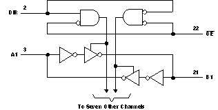
9.2 Functional Block Diagram
 Figure 2. Logic Diagram (Positive Logic)
9.3 Feature Description
9.3.1 Fully Configurable Dual-Rail Design Allows Each Port to Operate Over the Full 1.65-V to 5.5-V Power-Supply Range
Both VCCA and VCCB can be supplied at any voltage between 1.65 V and 5.5 V making the device suitable for translating between any of the voltage nodes (1.8 V, 2.5 V, 3.3 V and 5 V).
9.3.2 Ioff Supports Partial-Power-Down Mode Operation
Ioff prevents backflow current by disabling I/O output circuits when device is in partial-power-down mode.
9.4 Device Functional Modes
The SN74LVC8T245-EP is voltage level translator that can operate from 1.65 V to 5.5 V (VCCA) and 1.65 V to 5.5 V (VCCB). The signal translation between 1.65 V and 5.5 V requires direction control and output enable control. When OE is low and DIR is high, data transmission is from A to B. When OE is low and DIR is low, data transmission is from B to A. When OE is high, both output ports will be high-impedance.
Table 1. Function Table(1)
(Each 8-Bit Section)
| CONTROL INPUTS | OUTPUT CIRCUITS | OPERATION | ||
|---|---|---|---|---|
| OE | DIR | A PORT | B PORT | |
| L | L | Enabled | Hi-Z | B data to A bus |
| L | H | Hi-Z | Enabled | A data to B bus |
| H | X | Hi-Z | Hi-Z | Isolation |