SCES635B JULY 2005 – April 2015 SN74LVCH16T245
PRODUCTION DATA.
- 1 Features
- 2 Applications
- 3 Description
- 4 Revision History
- 5 Description (continued)
- 6 Pin Configuration and Functions
-
7 Specifications
- 7.1 Absolute Maximum Ratings
- 7.2 ESD Ratings
- 7.3 Recommended Operating Conditions
- 7.4 Thermal Information
- 7.5 Electrical Characteristics
- 7.6 Switching Characteristics for VCCA = 1.8 V ±0.15 V
- 7.7 Switching Characteristics for VCCA = 2.5 V ±0.2 V
- 7.8 Switching Characteristics for VCCA = 3.3 V ±0.3 V
- 7.9 Switching Characteristics for VCCA = 5 V ±0.5 V
- 7.10 Operating Characteristics
- 7.11 Typical Characteristics
- 8 Parameter Measurement Information
- 9 Detailed Description
- 10Application and Implementation
- 11Power Supply Recommendations
- 12Layout
- 13Device and Documentation Support
- 14Mechanical, Packaging, and Orderable Information
Package Options
Mechanical Data (Package|Pins)
Thermal pad, mechanical data (Package|Pins)
Orderable Information
12 Layout
12.1 Layout Guidelines
To ensure reliability of the device, following common printed-circuit-board layout guidelines is recommended.
- Bypass capacitors should be used on power supplies.
- Short trace lengths should be used to avoid excessive loading.
- Placing pads on the signal paths for loading capacitors or pullup resistors to help adjust rise and fall times of signals depending on the system requirements.
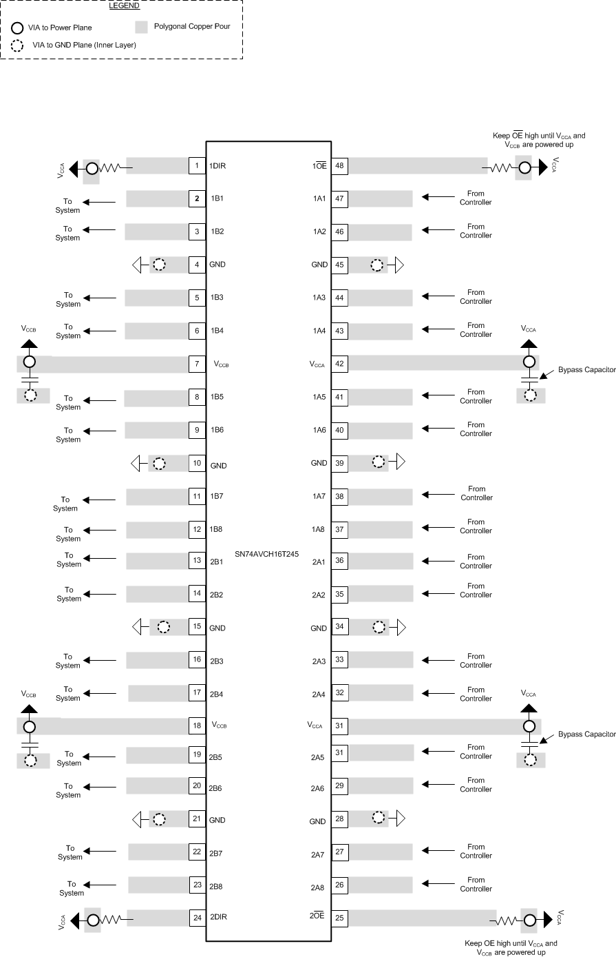
12.2 Layout Example
 Figure 6. SN74LVCH16T245 Layout Example