SCES008Q July 1995 – September 2018 SN54LVCH245A , SN74LVCH245A
PRODUCTION DATA.
- 1 Features
- 2 Applications
- 3 Description
- 4 Revision History
- 5 Pin Configuration and Functions
-
6 Specifications
- 6.1 Absolute Maximum Ratings
- 6.2 ESD Ratings
- 6.3 Recommended Operating Conditions: SN74LVCH245A
- 6.4 Recommended Operating Conditions: SN54LVCH245A
- 6.5 Thermal Information
- 6.6 Electrical Characteristics: SN74LVCH245A
- 6.7 Electrical Characteristics: SN54LVCH245A
- 6.8 Switching Characteristics: SN74LVCH245A, –40°C TO 85°C
- 6.9 Switching Characteristics: SN74LVCH245A, –40°C TO 125°C
- 6.10 Switching Characteristics: SN54LVCH245A
- 6.11 Operating Characteristics
- 6.12 Typical Characteristics
- 7 Parameter Measurement Information
- 8 Detailed Description
- 9 Application and Implementation
- 10Power Supply Recommendations
- 11Layout
- 12Device and Documentation Support
- 13Mechanical, Packaging, and Orderable Information
Package Options
Refer to the PDF data sheet for device specific package drawings
Mechanical Data (Package|Pins)
- DGV|20
- DB|20
- NS|20
- DW|20
- PW|20
- RGY|20
Thermal pad, mechanical data (Package|Pins)
Orderable Information
8.3.4 Bus-Hold Data Inputs
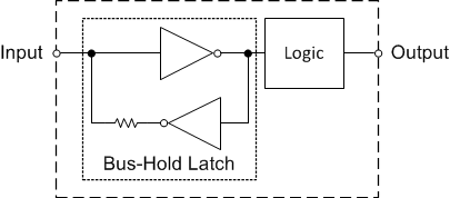
Each data input on this device includes a weak latch that maintains a valid logic level on the input. The state of these latches is unknown at startup and remains unknown until the input has been forced to a valid high or low state. After data has been sent through a channel, the latch then maintains the previous state on the input if the line is left floating.
NOTE
It is highly recommended to not use pull-up or pull-down resistors together with a bus-hold input.
Bus-hold data inputs prevent floating inputs on this device. The Implications of Slow or Floating CMOS Inputs application report explains the problems associated with leaving CMOS inputs floating.
These latches remain active at all times, independent of output disable signals such as direction selection or output enables.
The Bus-Hold Circuit application report has additional details regarding bus-hold inputs.
 Figure 9. Simplified Schematic For Device With Bus-Hold Data Inputs