SLLS144F October 1980 – October 2023 SN55173 , SN75173
PRODUCTION DATA
- 1
- 1 Features
- 2 Applications
- 3 Description
- 4 Pin Configuration and Functions
- 5 Specifications
- 6 Parameter Measurement Information
- 7 Detailed Description
- 8 Application and Implementation
- 9 Device and Documentation Support
- 10Revision History
- 11Mechanical, Packaging, and Orderable Information
Package Options
Refer to the PDF data sheet for device specific package drawings
Mechanical Data (Package|Pins)
- NS|16
- N|16
- D|16
Thermal pad, mechanical data (Package|Pins)
- D|16
Orderable Information
3 Description
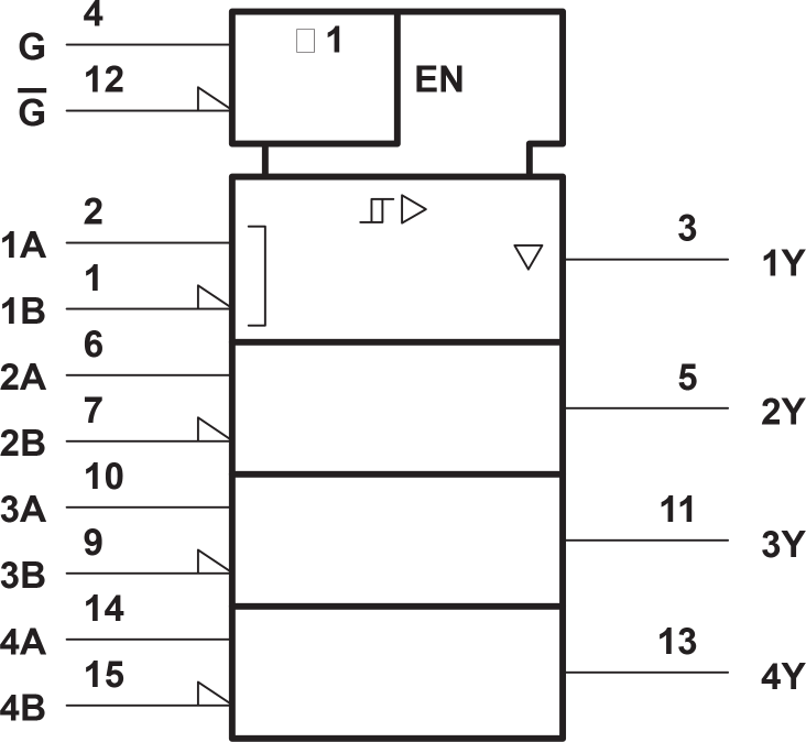
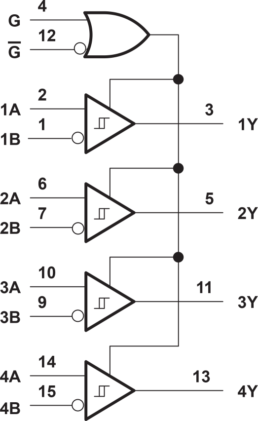
The SN55173 and SN75173 are monolithic quadruple differential line receivers with 3-state outputs. They are designed to meet the requirements of TIA/EIA-422-B, TIA/EIA-423-B, TIA/EIA-485-A, and several ITU recommendations. The standards are for balanced multipoint bus transmission at rates up to 10 megabits per second. The four receivers share two OR enable inputs, one active when high, the other active when low. These devices feature high input impedance, input hysteresis for increased noise immunity, and input sensitivity of ± 200 mV over a common-mode input voltage range of – 12 V to 12 V. Fail-safe design specifies that if the inputs are open circuited, the outputs are always high. The SN65173 and SN75173 are designed for optimum performance when used with the SN75172 or SN75174 quad differential line drivers.
The SN55173 is characterized over the full military temperature range of – 55°C to 125°C. The SN75173 is characterized for operation from 0°C to 70°C.
| PART NUMBER | PACKAGE(1) | PACKAGE SIZE(2) |
|---|---|---|
| SN55173 | J (CDIP, 16) | 6.92 mm × 19.56 mm |
| FK (LCCC, 20)(3) | 8.89 mm × 8.89 mm | |
| SN75173 | D (SOIC, 16) | 9.9 mm × 6 mm |
| N (PDIP, 16) | 19.3 × 9.4 mm | |
| NS (SO, 16) | 10.2 × 7.8 mm |

 Logic Diagram (Positive Logic)