SLLS378E May   2000  – January 2023 SN65LBC180A , SN75LBC180A

PRODUCTION DATA  

  1. 1Features
  2. 2Description
  3. 3Revision History
  4. 4Pin Configuration and Functions
  5. 5Reference
    1. 5.1 Absolute Maximum Ratings
    2. 5.2 Dissipation Ratings
    3. 5.3 RECOMMENDED OPERATING CONDITIONS
    4. 5.4 Thermal Information
    5. 5.5 Driver Electrical Characteristics
    6. 5.6 Driver Switching Characteristics
    7. 5.7 Receiver Electrical Characteristics
    8. 5.8 Receiver Switching Characteristics
    9.     Typical Characteristics
      1.      Parameter Measurement Information
  6. 6Detailed Description
    1. 6.1 Device Functional Modes
      1. 6.1.1 Functional Tables
      2. 6.1.2 Schematics of Inputs and Outputs
  7. 7Application Information
    1. 7.1 Typical Application Circuit
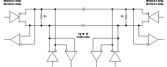
  8. 8Device and Documentation Support
    1. 8.1 Receiving Notification of Documentation Updates
    2. 8.2 Support Resources
    3. 8.3 Trademarks
    4. 8.4 Electrostatic Discharge Caution
    5. 8.5 Glossary
  9. 9Mechanical, Packaging, and Orderable Information

Package Options

Refer to the PDF data sheet for device specific package drawings

Mechanical Data (Package|Pins)
  • N|14
Thermal pad, mechanical data (Package|Pins)
Orderable Information

Typical Application Circuit

GUID-9D7DFD5A-28F0-48D4-B9A8-4547051DF3F2-low.gif
The line should be terminated at both ends in its characteristic impedance (RT = ZO). Stub lengths off the main line should be kept as short as possible. One SN65LBC180A typically represents less than one unit load.