SLLSE41H June 2010 – March 2016 SN75LVCP601
PRODUCTION DATA.
- 1 Features
- 2 Applications
- 3 Description
- 4 Revision History
- 5 Pin Configuration and Functions
- 6 Specifications
- 7 Parameter Measurement Information
- 8 Detailed Description
- 9 Application and Implementation
- 10Power Supply Recommendations
- 11Layout
- 12Device and Documentation Support
- 13Mechanical, Packaging, and Orderable Information
Package Options
Mechanical Data (Package|Pins)
- RTJ|20
Thermal pad, mechanical data (Package|Pins)
- RTJ|20
Orderable Information
6 Specifications
6.1 Absolute Maximum Ratings
over operating free-air temperature range (unless otherwise noted)(1)| MIN | MAX | UNIT | ||
|---|---|---|---|---|
| VCC | Supply voltage range(2) | –0.5 | 4 | V |
| Voltage range | Differential I/O | –0.5 | 4 | V |
| Control I/O | –0.5 | VCC + 0.5 | V | |
| Continuous power dissipation | See Power Dissipation Characteristics | |||
| Tstg | Storage temperature | 150 | °C | |
(1) Stresses beyond those listed under Absolute Maximum Ratings may cause permanent damage to the device. These are stress ratings only, and functional operation of the device at these or any conditions beyond those indicated under Recommended Operating Conditions is not implied. Exposure to absolute-maximum-rated conditions for extended periods may affect device reliability.
(2) All voltage values, except differential voltages, are with respect to the network ground terminal.
6.2 ESD Ratings
| VALUE | UNIT | |||
|---|---|---|---|---|
| V(ESD) | Electrostatic discharge | Human body model (HBM), per ANSI/ESDA/JEDEC JS-001(1) | ±10000 | V |
| Charged-device model (CDM), per JEDEC specification JESD22-C101(2) | ±1500 | |||
| Machine model(3) | ±200 | |||
(1) JEDEC document JEP155 states that 500-V HBM allows safe manufacturing with a standard ESD control process.
(2) JEDEC document JEP157 states that 250-V CDM allows safe manufacturing with a standard ESD control process.
(3) Tested in accordance with JEDEC Standard 22, Test Method A115-A.
6.3 Recommended Operating Conditions
typical values for all parameters are VCC = 3.3 V and TA = 25°C; all temperature limits are specified by design| MIN | NOM | MAX | UNIT | ||
|---|---|---|---|---|---|
| VCC | Supply voltage | 3 | 3.3 | 3.6 | V |
| CCOUPLING | Coupling capacitor | 12 | nF | ||
| Operating free-air temperature | 0 | 85 | °C | ||
6.4 Thermal Information
| THERMAL METRIC(1) | SN75LVCP601 | UNIT | |
|---|---|---|---|
| RTJ (WQFN) | |||
| 20 PINS | |||
| RθJA | Junction-to-ambient thermal resistance | 38 | °C/W |
| RθJC(top) | Junction-to-case (top) thermal resistance | 40 | °C/W |
| RθJB | Junction-to-board thermal resistance | 10 | °C/W |
| ψJT | Junction-to-top characterization parameter | 0.5 | °C/W |
| ψJB | Junction-to-board characterization parameter | 0.9 | °C/W |
| RθJC(bot) | Junction-to-case (bottom) thermal resistance | 15.2 | °C/W |
(1) For more information about traditional and new thermal metrics, see the Semiconductor and IC Package Thermal Metrics application report, SPRA953.
6.5 Electrical Characteristics
over operating free-air temperature range (unless otherwise noted)| PARAMETER | TEST CONDITIONS | MIN | TYP | MAX | UNIT | |
|---|---|---|---|---|---|---|
| DEVICE PARAMETERS | ||||||
| PD | Power dissipation in active mode | DEWx = EN = VCC, EQx = DEx = NC, K28.5 pattern at 6 Gbps, VID = 700 mVp-p | 215 | 288 | mW | |
| PSD | Power dissipation in standby mode | EN = 0 V, DEWx = EQx = DEx = NC, K28.5 pattern at 6 Gbps, VID = 700 mVp-p | 5 | mW | ||
| ICC | Active-mode supply current | EN = 3.3 V, DEWx = 0 V, EQx = DEx = NC, K28.5 pattern at 6 Gbps, VID = 700 mVp-p |
65 | 80 | mA | |
| ICC_ALP | Acive power-save mode ICC | When device is enabled and auto low-power conditions are met | 6.5 | 10 | mA | |
| ICC_STDBY | Standby mode supply current | EN = 0 V | 1 | mA | ||
| Maximum data rate | 1 | 6 | Gbps | |||
| OUT-OF-BAND (OOB) | ||||||
| VOOB | Input OOB threshold | f = 750 MHz | 50 | 78 | 150 | mVpp |
| DVdiffOOB | OOB differential delta | 25 | mV | |||
| DVCMOOB | OOB common-mode delta | 50 | mV | |||
| CONTROL LOGIC | ||||||
| VIH | Input high voltage | For all control pins | 1.4 | V | ||
| VIL | Input low voltage | 0.5 | V | |||
| VINHYS | Input hysteresis | 115 | mV | |||
| IIH | High-level input current | EQx, DEx = VCC | 30 | µA | ||
| EN, DEWx = VCC | 1 | |||||
| IIL | Low-level input current | EQx, DEx = GND | –30 | µA | ||
| EN, DEWx = GND | –10 | |||||
| RECEIVER AC/DC | ||||||
| ZDIFFRX | Differential-input impedance | 85 | 100 | 115 | Ω | |
| ZSERX | Single-ended input impedance | 40 | Ω | |||
| VCMRX | Common-mode voltage | 1.8 | V | |||
| RLDiffRX | Differential-mode return loss (RL) | f = 150 MHz to 300 MHz | 18 | 28 | dB | |
| f = 300 MHz to 600 MHz | 14 | 17 | ||||
| f = 600 MHz to 1.2 GHz | 10 | 12 | ||||
| f = 1.2 GHz to 2.4 GHz | 8 | 9 | ||||
| f = 2.4 GHz to 3 GHz | 3 | 9 | ||||
| RXDiffRLSlope | Differential-mode RL slope | f = 300 MHz to 6 GHz (see Figure 1) | –13 | dB/dec | ||
| RLCMRX | Common-mode return loss | f = 150 MHz to 300 MHz | 5 | 10 | dB | |
| f = 300 MHz to 600 MHz | 5 | 17 | ||||
| f = 600 MHz to 1.2 GHz | 2 | 23 | ||||
| f = 1.2 GHz to 2.4 GHz | 1 | 16 | ||||
| f = 2.4 GHz to 3 GHz | 1 | 12 | ||||
| VdiffRX | Differential input voltage PP | f = 1.5 GHz and 3 GHz | 120 | 1600 | mVppd | |
| IBRX | Impedance balance | f = 150 MHz to 300 MHz | 30 | 41 | dB | |
| f = 300 MHz to 600 MHz | 30 | 38 | ||||
| f = 600 MHz to 1.2 GHz | 20 | 32 | ||||
| f = 1.2 GHz to 2.4 GHz | 10 | 26 | ||||
| f = 2.4 GHz to 3 GHz | 10 | 25 | ||||
| f = 3 GHz to 5 GHz | 4 | 20 | ||||
| f = 5 GHz to 6.5 GHz | 4 | 17 | ||||
| TRANSMITTER AC/DC | ||||||
| ZdiffTX | Pair differential impedance | 85 | 100 | 122 | Ω | |
| ZSETX | Single-ended impedance | 40 | Ω | |||
| VTXtrans | Sequencing transient voltage | Transient voltages on the serial data bus during power sequencing (lab load) | –1.2 | 1.2 | V | |
| RLDiffTX | Differential-mode return loss | f = 150 MHz to 300 MHz | 14 | 24 | dB | |
| f = 300 MHz to 600 MHz | 8 | 19 | ||||
| f = 600 MHz to 1.2 GHz | 6 | 14 | ||||
| f = 1.2 GHz to 2.4 GHz | 6 | 10 | ||||
| f = 2.4 GHz to 3 GHz | 3 | 10 | ||||
| TXDiffRLSlope | Differential-mode RL slope | f = 300 MHz to 3 GHz (see Figure 1) | –13 | dB/dec | ||
| RLCMTX | Common-mode return loss | f = 150 MHz to 300 MHz | 5 | 20 | dB | |
| f = 300 MHz to 600 MHz | 5 | 19 | ||||
| f = 600 MHz to 1.2 GHz | 2 | 17 | ||||
| f = 1.2 GHz to 2.4 GHz | 1 | 12 | ||||
| f = 2.4 GHz to 3.0 GHz | 1 | 11 | ||||
| IBTX | Impedance balance | f = 150 MHz to 300 MHz | 30 | 41 | dB | |
| f = 300 MHz to 600 MHz | 30 | 38 | ||||
| f = 600 MHz to 1.2 GHz | 20 | 33 | ||||
| f = 1.2 GHz to 2.4 GHz | 10 | 24 | ||||
| f = 2.4 GHz to 3 GHz | 10 | 26 | ||||
| f = 3 GHz to 5 GHz | 4 | 22 | ||||
| f = 5 GHz to 6.5 GHz | 4 | 21 | ||||
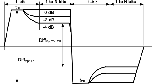
| DE | Output de-emphasis (relative to transition bit) | f = 3 GHz, DE1 or DE2 = 0 | 0 | dB | ||
| f = 3 GHz, DE1 or DE2 = 1 | –2 | |||||
| f = 3 GHz, DE1 or DE2 = NC | –4 | |||||
| DiffVppTX_DE | Differential output-voltage swing dc level | f = 3 GHz, DE1 or DE2 = 0 | 550 | mV | ||
| f = 3 GHz, DE1 or DE2 = 1 | 830 | |||||
| f = 3 GHz, DE1or DE2 = NC | 630 | |||||
| VCMAC_TX | TX AC CM voltage | At 1.5 GHz | 20 | 50 | mVppd | |
| At 3 GHz | 12 | 26 | dBmV (rms) | |||
| At 6 GHz | 13 | 30 | ||||
| VCMTX | Common-mode voltage | 1.8 | V | |||
| TxR/FImb | TX rise-fall imbalance | At 3 Gbps | 6% | 20% | ||
| TxAmpImb | TX amplitude imbalance | 2% | 10% | |||
(1) TJ = (14.1 × RJSD + DJ), where RJSD is one standard deviation value of RJ Gaussian distribution. Jitter measurement is at the SATA connector and includes jitter generated at the package connection on the printed circuit board, and at the board interconnect as shown in Figure 9.
6.6 Power Dissipation Characteristics
over operating free-air temperature range (unless otherwise noted)| PARAMETER | MIN | MAX | UNIT | ||
|---|---|---|---|---|---|
| PD | Device power dissipation in active mode | 215 | 288 | mW | |
| PSD | Device power dissipation under standby mode | 5 | mW | ||
6.7 Timing Requirements
| MIN | NOM | MAX | UNIT | |||
|---|---|---|---|---|---|---|
| DEVICE PARAMETERS | ||||||
| AutoLPENTRY | Auto low-power entry time | Electrical idle at input (see Figure 4) | 80 | 105 | 130 | µs |
| AutoLPEXIT | Auto low-power exit time | After first signal activity (see Figure 4) | 42 | 50 | ns | |
| TRANSMITTER AC/DC | ||||||
| tDE | De-emphasis duration | DEW1 or DEW2 = 0 | 94 | ps | ||
| DEW1 or DEW2 = 1 | 215 | |||||
| OUT-OF-BAND (OOB) | ||||||
| tOOB1 | OOB mode enter | See Figure 4 | 3 | 5 | ns | |
| tOOB2 | OOB mode exit | See Figure 4 | 3 | 5 | ns | |
6.8 Switching Characteristics
over operating free-air temperature range (unless otherwise noted)| PARAMETER | TEST CONDITIONS | MIN | TYP | MAX | UNIT | |
|---|---|---|---|---|---|---|
| DEVICE PARAMETERS | ||||||
| tPDelay | Propagation delay | Measured using K28.5 pattern (see Figure 2) | 323 | 400 | ps | |
| tENB | Device enable time | EN 0 → 1 | 5 | µs | ||
| tDIS | Device disable time | EN 1 → 0 | 2 | µs | ||
| RECEIVER AC/DC | ||||||
| t20-80RX | Rise/fall time | Rise times and fall times measured between 20% and 80% of the signal. SATA 6-Gbps speed measured 1 in, (2.5 cm) from device pin. | 62 | 75 | ps | |
| tskewRX | Differential skew | Difference between the single-ended midpoint of the RX+ signal rising or falling edge, and the single-ended midpoint of the RX– signal falling or rising edge. | 30 | ps | ||
| TRANSMITTER AC/DC | ||||||
| t20-80TX | Rise/fall time | Rise times and fall times measured between 20% and 80% of the signal. At 6 Gbps under no load conditions. | 42 | 55 | 75 | ps |
| tskewTX | Differential skew | Difference between the single-ended mid-point of the TX+ signal rising or falling edge, and the single-ended mid-point of the TX– signal falling or rising edge. | 6 | 20 | ps | |
| TRANSMITTER JITTER | ||||||
| DJTX | Deterministic jitter(1) at CP in Figure 9 | VID = 500 mVpp, UI = 333 ps, K28.5 control character |
0.06 | 0.07 | UIp-p | |
| RJTX | Residual random jitter(1) | VID = 500 mVpp, UI = 333 ps, K28.7 control character |
0.01 | 2 | ps-rms | |
| DJTX | Deterministic jitter(1) at CP in Figure 9 | VID = 500 mVpp, UI = 167 ps, K28.5 control character |
0.08 | 0.16 | UIp-p | |
| RJTX | Residual random jitter(1) | VID = 500 mVpp, UI = 167 ps, K28.7 control character |
0.09 | 2 | ps-rms | |
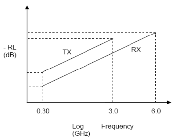 Figure 1. TX, RX Differential Return Loss Limits
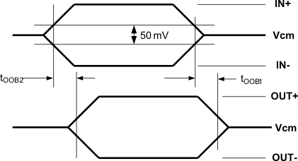 Figure 2. OOB Enter and Exit Timing
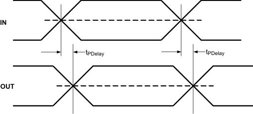 Figure 3. Propagation Delay Timing Diagram
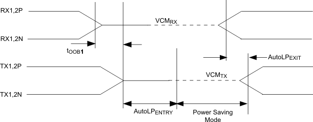 Figure 4. Auto Low-Power Mode Enter and Exit Timing
6.9 Typical Characteristics
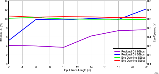 Figure 6. Residual DJ and Eye Opening
 vs Input Trace Length
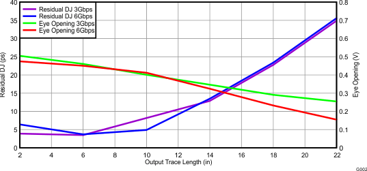 Figure 7. Residual DJ and Eye Opening
 vs Output Trace Length
