SLLSEW8 September 2016 SN75LVPE801
PRODUCTION DATA.
- 1 Features
- 2 Applications
- 3 Description
- 4 Revision History
- 5 Description (continued)
- 6 Pin Configuration and Functions
- 7 Specifications
- 8 Parameter Measurement Information
- 9 Detailed Description
- 10Applications and Implementation
- 11Power Supply Recommendations
- 12Layout
- 13Device and Documentation Support
- 14Mechanical, Packaging, and Orderable Information
Package Options
Mechanical Data (Package|Pins)
- DRF|8
Thermal pad, mechanical data (Package|Pins)
- DRF|8
Orderable Information
1 Features
- SATA Express Support
- Selectable Equalization and De-Emphasis
- Hot Plug Capable
- Receiver Detect and OOB Support
- Multirate Operation
- SATA: 1.5 Gpbs, 3.0 Gpbs, 6.0 Gpbs
- PCIe: 2.5 Gbps, 5.0 Gbps, 8.0 Gbps
- Suitable to Receive 8.0 Gbps Data Over Up to 40 Inches (1.0 Meter) of FR4 PC Board
- Compensates Up to 14-dB Loss on the Receive Side and 1.2dB Loss on the Transmit Side at
3 GHz - Integrated Output Squelch
- Temperature range 0°C – 85°C
- Auto Low Power Feature Lowers Power by > 90%
- < 100 mW (Active Mode, Typical)
- < 11 mW (Auto Low Power Mode, Typical)
- Single 3.3-V Supply
- High Protection Against ESD Transient
- HBM: 6 kV
- CDM: 1.5 kV
- Ultra-Small Footprint: 2 mm × 2 mm WSON Package
2 Applications
- Notebooks
- Desktops
- Docking Stations
- Servers
- Workstations
3 Description
The SN75LVPE801 is a versatile single channel, SATA Express signal conditioner supporting data rates up to 8 Gbps. The device supports SATA Gen 1, 2, and 3 specifications as well as PCIe 1.0, 2.0, and 3.0. The SN75LVPE801 operates from a single 3.3-V supply and has 100-Ω line termination with self-biasing feature, making the device suitable for AC coupling. The inputs incorporate an out-of-band (OOB) detector, which automatically squelches the output when the input differential voltage falls below threshold while maintaining a stable common-mode voltage. The device is also designed to handle spread spectrum clocking (SSC) transmission per SATA standard.
The SN75LVPE801 handles interconnect losses at its input with selectable equalization settings that can be programmed to match the loss in the channel. For data rates of 8 Gbps and lower the SN75LVPE801 equalizes signals for a span of up to 50 inches of FR4 board material. For data rates of 8 Gbps the device compensates up to 40 in of FR4 material. The equalization level is controlled by the setting of the signal control pin EQ.
Device Information(1)
| PART NUMBER | PACKAGE | BODY SIZE (NOM) |
|---|---|---|
| SN75LVPE801 | WSON (8) | 2.00 mm × 2.00 mm |
- For all available packages, see the orderable addendum at the end of the data sheet.
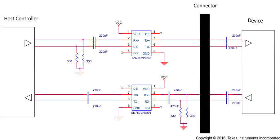
SATA Express Reference Schematic
