SLLSEW8 September 2016 SN75LVPE801
PRODUCTION DATA.
- 1 Features
- 2 Applications
- 3 Description
- 4 Revision History
- 5 Description (continued)
- 6 Pin Configuration and Functions
- 7 Specifications
- 8 Parameter Measurement Information
- 9 Detailed Description
- 10Applications and Implementation
- 11Power Supply Recommendations
- 12Layout
- 13Device and Documentation Support
- 14Mechanical, Packaging, and Orderable Information
Package Options
Mechanical Data (Package|Pins)
- DRF|8
Thermal pad, mechanical data (Package|Pins)
- DRF|8
Orderable Information
12 Layout
12.1 Layout Guidelines
12.1.1 Return Current and Plane References
High frequency return signal/current is defined as the path that a signal follows back to its original source as all signals flow in a closed loop. Minimizing the loop area of the closed loop is beneficial for both EMI (Electro-Magnetic Interference) reduction and signal integrity.
The best way to minimize loop area is to always have a signal reference their nearest solid ground or power plane. Obstructions to the return signal causes signal integrity problems like reflections, crosstalk, undershoot and overshoot.
Signals can reference either power or ground planes, but ground is preferred. Without solid plane references, single ended and differential impedance control is very hard to accomplish; crosstalk to other signals may happen as the return signals have no other path. This type of crosstalk is difficult to troubleshoot.
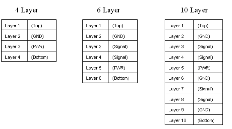
Symmetric pairing of solid planes in the layer stackup can significantly reduce warping of the PCB during the manufacturing process. Warping of the PCB is crucial to minimize on boards that uses BGA components.
12.1.2 Split Planes – What to Avoid
Never route signals over splits in their perspective reference planes.
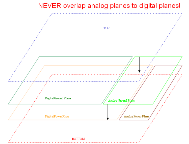 Figure 28. Overlapping Analog and Digital Planes
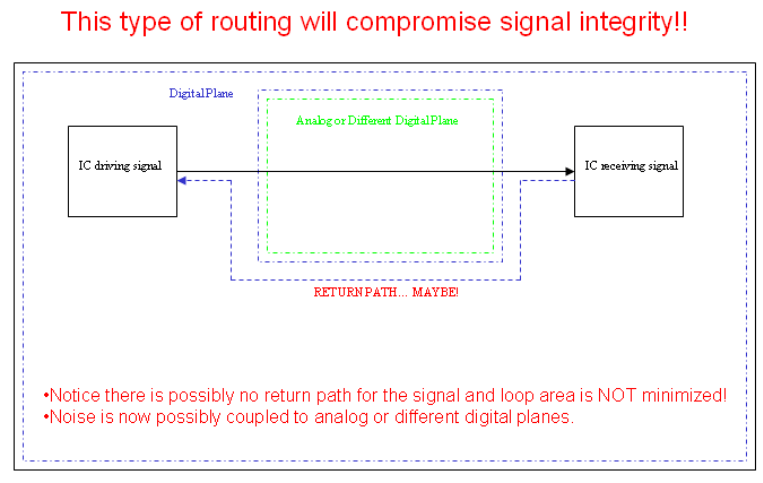 Figure 29. Incorrect Routing
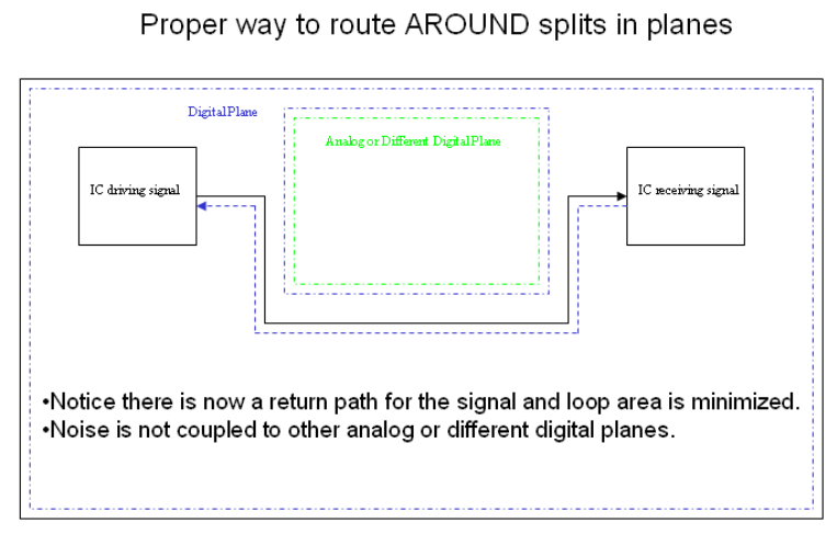 Figure 30. Proper Routing
12.1.3 Avoiding Crosstalk
Crosstalk is defined as interference from one trace to another by either or both inductive and capacitive coupling. Best ways to avoid crosstalk are:
- Provide stable reference planes for all high speed signals (as noted in previous sections).
- Use the 3W rule (3 times the width of trace for separation) where applicable on all signals, but absolutely use on clock signals.
- Use ground traces/guards around either victim or aggressor signals prone to crosstalk.
- When space is constrained and limited on areas of the PCB to route parallel buses, series or end termination resistors can be used to route traces closer than what is normally recommended. However, calculations and simulations must be done to validate the use of series or end termination resistors to eliminate crosstalk.
 Figure 31. Ways to Avoid Crosstalk
12.2 Layout Example
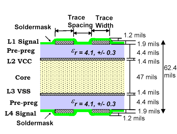 Figure 32. Printed-Circuit Board Stackup (FR-4 Example)
