SLLSEW8 September 2016 SN75LVPE801
PRODUCTION DATA.
- 1 Features
- 2 Applications
- 3 Description
- 4 Revision History
- 5 Description (continued)
- 6 Pin Configuration and Functions
- 7 Specifications
- 8 Parameter Measurement Information
- 9 Detailed Description
- 10Applications and Implementation
- 11Power Supply Recommendations
- 12Layout
- 13Device and Documentation Support
- 14Mechanical, Packaging, and Orderable Information
Package Options
Mechanical Data (Package|Pins)
- DRF|8
Thermal pad, mechanical data (Package|Pins)
- DRF|8
Orderable Information
9 Detailed Description
9.1 Overview
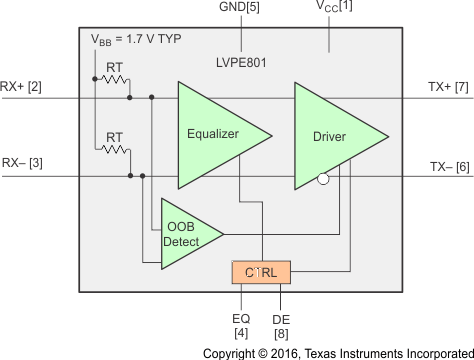
The SN75LVPE801 is a single channel equalizer and redriver. The device operates over a wide range of signaling rates, supporting operation from DC to 8 Gbps. The wide operating range supports SATA Gen 1,2,3 (1.5 Gbps, 3.0 Gbps, and 6.0 Gbps respectively) as well as PCI Express 1.0, 2.0, 3.0 (2.5 Gbps, 5.0 Gbps, and 8.0 Gbps). The device also supports SATA Express (SATA 3.2) which is a form factor specification that allows for SATA and PCI Express signaling over a single connector.
9.2 Functional Block Diagram

9.3 Feature Description
9.3.1 SATA Express
SATA Express (sometimes SATAe) is an electro-mechanical standard that supports both SATA and PCI Express storage devices. SATAe is standardized in the SATA 3.2 standard. The standard is concerned with providing a smooth transition from SATA to PCIe storage devices. The standard provides for standardized cables and connectors, and muxes the PCIe and SATA lanes at the host side so that either SATA compliant or PCIe compliant devices may operate with a host.
SATAe provides support for SATA1, SATA2 and SATA3 devices (operating from 1.5 Gbps to 6.0 Gbps), as well as PCIe1, PCIe2 and PCIe3 devices (operating from 2.5 Gbps to 8.0 Gbps).
The SN75LVPE801 provides for equalization and re-drive of a single channel input signal complying with any of the SATA or PCIe standards available with SATAe.
The SATAe standard provides for a mechanism for a host to recognize and detect whether a SATA or PCIe device is plugged into the host. See the Typical SATA Applications section for the details of the SATA Express Interface Detect operation.
9.3.2 Receiver Termination
The receiver has integrated terminations to an internal bias voltage. The receiver differential input impedance is nominally 100 Ω, with a ±15% variation.
For PCI Express compatibility it is necessary to include 330 Ω pull-down resistors between the connector and the AC capacitors, refer to Figure 24 for more information.
9.3.3 Receiver Internal Bias
The SN75LVPE801 receiver is internally biased to 1.7 V, providing support for AC coupled inputs.
9.3.4 Receiver Equalization
The SN75LVPE801 incorporates programmable equalization. The EQ input controls the level of equalization that is used to open the eye of the received input signal. If the EQ input is left open, or pulled LO, 8 dB (at 4 GHz) of equalization is applied. When the EQ input is HIGH, the equalization is set to 16 dB (again at 4 GHz).Table 1 shows the equalization values discussed.
Table 1. EQ and DE Settings
| EQ | EQUALIZATION dB (at 8 Gbps) |
DE | DE-EMPHASIS |
|---|---|---|---|
| 0 (default) | 8 | 0 (default) | 0 |
| 1 | 16 | 1 | –1.2 |
9.3.5 OOB/Squelch
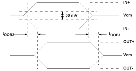
The SN75LVPE801 receiver incorporates an Out-Of-Band (OOB) detection circuit in addition to the main signal chain receiver. The OOB detector continuously monitors the differential input signal to the device. The OOB detector has a 50-mVpp entry threshold. If the differential signal at the receiver input is less than the OOB entry threshold, the device transmitter transitions to squelch. The SN75LVPE801 enters squelch within 5 ns of the input signal falling below the OOB entry threshold. The SN75LVPE801 continues to monitor the input signal while in squelch. While in squelch, if the OOB detector determines that the input signal now exceeds the 90 mVpp exit threshold, the SN75LVPE801 exits squelch within 5 ns. See Figure 8.
 Figure 8. OOB Enter and Exit Timing
Receiver Input Termination is Disabled
When the SN75LVPE801 enters squelch state the transmitter output is squelched. The transmitter non-inverting (TX+) output and the transmitter inverting output (TX-) are both driven to the transmitter nominal common mode voltage which is 1.7 V .
9.3.6 Auto Low Power
The SN75LVPE801 also includes an Auto Low Power Mode (ALP). ALP is entered when the differential input signal has been less than 50 mV for > 10 µs. The device enters and exits Low Power Mode by actively monitoring the input signal level. In this state the device selectively shuts off internal circuitry to lower power by > 90% of its normal operating power. While in ALP mode the device continues to actively monitor input signal levels. When the input signal exceeds the OOB exit threshold level, the device reverts to the active state. Exit time from Auto Low Power Mode is < 50 ns (max). See Figure 9.
 Figure 9. Auto Low Power Mode Entry and Exit Timing
9.3.7 Transmitter Output Signal
The SN75LVPE801 differential output signal is 650 mVpp when de-emphasis is disabled (DE input is open or pulled low).
9.3.8 Transmitter Common Mode
The SN75LVPE801 transmitter common mode output is set to 1.7 V.
9.3.9 De-Emphasis
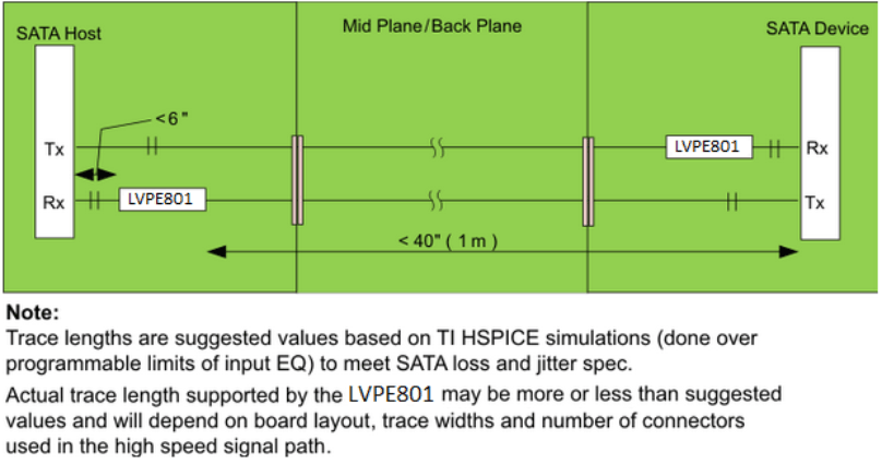
The SN75LVPE801 transmitter incorporates programmable de-emphasis to provide signal conditioning to offset the anticipated channel losses based on expected use cases for the device. Figure 10 shows an example of a SATA host communicating with a SATA device through a backplane. In such a use case, an SN75LVPE801 would be located at the end of the interconnect channels (i.e. at the device end for the host TX channel, and at the host end for the host RX channel. These locations are selected based on the signal conditioning that is incorporated into the SN75LVPE801. The SN75LVPE801 provides up to 16 dB of equalization, while supporting up to 1.2 dB of de-emphasis. The optimum location would therefore be at the end of the interconnect, allowing the receiver equalization to address the majority of the channel loss, while the de-emphasis would be employed to overcome the much shorter interconnect length.
The DE input controls the amount of de-emphasis that is applied at the transmitter output. The de-emphasis selections are shown in Table 1. When DE is left open, or pulled low, de-emphasis shall be off. When DE is pulled HIGH, 1.2 dB of de-emphasis is used at the transmitter output.
 Figure 10. Trace Length Example
9.3.10 Transmitter Termination
The SN75LVPE801 transmitter includes integrated terminations. The receiver differential output impedance is nominally 100 Ω, with a ≤ 22% variation.
9.4 Device Functional Modes
9.4.1 Active
Active mode is the normal operating mode. When power is applied to the device, and the differential input signal to the receiver is greater than 90 mVpp, the device is in active mode and meets all the specifications in the data sheet.
9.4.2 Squelch
When the device is powered, and the differential input signal to the receiver is less than 50 mVpp, the device is in squelch mode. In squelch mode the transmitter outputs are both set to VCMTX or 1.7 V.
9.4.3 Auto Low Power
When the device is powered and the differential input signal to the receiver has been less than 50 mVpp for greater than 10 ns, the device transitions to Auto Low Power (ALP) mode. In ALP, the transmitter outputs are both set to VCMTX. In addition, while in ALP, the device shuts off internal circuitry to lower power to less than 10% of the power in the Active mode.