SLLSET1B January 2016 – February 2017 SN75LVPE802
PRODUCTION DATA.
- 1 Features
- 2 Applications
- 3 Description
- 4 Revision History
- 5 Description (continued)
- 6 Pin Configuration and Functions
- 7 Specifications
- 8 Detailed Description
- 9 Application and Implementation
- 10Power Supply Recommendations
- 11Layout
- 12Device and Documentation Support
- 13Mechanical, Packaging, and Orderable Information
Package Options
Refer to the PDF data sheet for device specific package drawings
Mechanical Data (Package|Pins)
- RTJ|20
Thermal pad, mechanical data (Package|Pins)
- RTJ|20
Orderable Information
1 Features
- SATA Express Support
- Selectable Equalization and De-Emphasis
- Hot Plug Capable
- Receiver Detect and OOB Support
- Integrated Output Squelch
- Multirate Operation
- SATA: 1.5 Gpbs, 3 Gpbs, 6 Gpbs
- PCIe: 2.5 Gbps, 5 Gbps, 8 Gbps
- Excellent Jitter and Loss Compensation Capability to Over 24-Inch (61-cm) FR4 Trace
- Low Power
- < 220 mW (Typical)
- < 50 mW (in Auto Low-Power Mode)
- < 5 mW (in Standby Mode)
- 20-Pin 4-mm × 4-mm QFN Package
- High Protection Against ESD Transient
- HBM: 10,000 V
- CDM: 1,500 V
- MM: 200 V
- Extended Commercial Temperature Support 0°C to 85°C
2 Applications
- Tablets
- Notebooks
- Desktops
- Docking Stations
3 Description
The SN75LVPE802 is a versatile dual channel, SATA Express signal conditioner supporting data rates up to 8 Gbps. The device supports SATA Gen 1, 2, and 3 specifications as well as PCIe 1, 2, 3. The SN75LVPE802 operates from a single 3.3-V supply and has 100-Ω line termination with self-biasing feature, making the device suitable for AC coupling. The inputs incorporate an out-of-band (OOB) detector, which automatically squelches the output when the input differential voltage falls below threshold while maintaining a stable common-mode voltage. The device is also designed to handle spread spectrum clocking (SSC) transmission per SATA standard.
The SN75LVPE802 handles interconnect losses at its input with selectable equalization settings that can be programmed to match the loss in the channel. For data rates of 3 Gbps and lower, the SN75LVPE802 equalizes signals for a span of up to 50 inches of FR4 board material. For data rates of 8 Gbps, the device compensates up to 40 in of FR4 material. The equalization level is controlled by the setting of the signal control pin EQ.
Two de-emphasis levels can be selected on the transmit side to provide 0 or 1.2 dB of additional high- frequency loss compensation at the output.
Device Information(1)
| PART NUMBER | PACKAGE | BODY SIZE (NOM) |
|---|---|---|
| SN75LVPE802 | WQFN (20) | 4.00 mm x 4.00 mm |
- For all available packages, see the orderable addendum at the end of the data sheet.
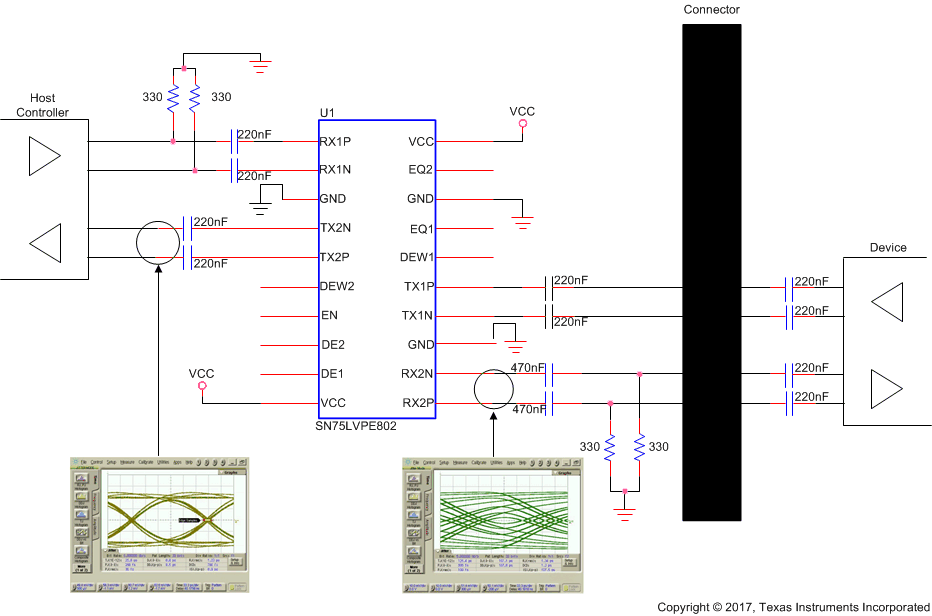
Simplified Schematics
