SBFS023C June 2003 – December 2016 SRC4190
PRODUCTION DATA.
- 1 Features
- 2 Applications
- 3 Description
- 4 Revision History
- 5 Pin Configuration and Functions
- 6 Specifications
- 7 Detailed Description
-
8 Application and Implementation
- 8.1 Application Information
- 8.2 Typical Application
- 9 Power Supply Recommendations
- 10Layout
- 11Device and Documentation Support
- 12Mechanical, Packaging, and Orderable Information
Package Options
Mechanical Data (Package|Pins)
- DB|28
Thermal pad, mechanical data (Package|Pins)
Orderable Information
8 Application and Implementation
NOTE
Information in the following applications sections is not part of the TI component specification, and TI does not warrant its accuracy or completeness. TI’s customers are responsible for determining suitability of components for their purposes. Customers should validate and test their design implementation to confirm system functionality.
8.1 Application Information
The audio input and output ports can handle 16-, 18-, 20-, or 24-bit right-justified PCM serial data, as well as
24-bit I2S or left-justified PCM serial data at up to 212-kHz sampling rate. A TDM format is also available. Both input and output can operate in slave mode, or one can operate as a master while the other operates as a slave. A 16:1 or 1:16 ratio is the maximum supported between the input and output audio sampling rates.
8.2 Typical Application
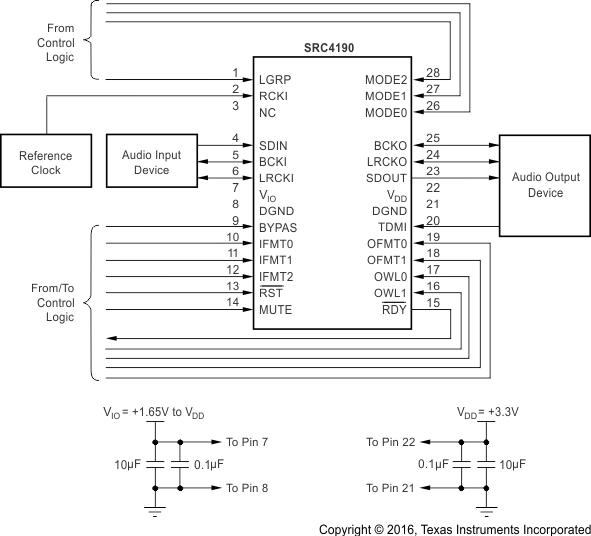 Figure 63. Typical Connection Diagram for the SRC4190
8.2.1 Design Requirements
For this design example, use the parameters listed in Table 4 as the input parameters.
Table 4. Design Parameters
| PARAMETER | VALUE |
|---|---|
| VDD supply voltage, VDD | 3.3 V |
| VIO supply voltage, VIO | 1.65 V to VDD |
| Bypass capacitors | 0.1 µF and 10 µF |
8.2.2 Detailed Design Procedure
The typical connection diagram for the SRC4190 is shown in Figure 63. Recommended values for power supply bypass capacitors are included. These capacitors must be placed as close to the IC package as possible.
8.2.2.1 Reference Clock
The SRC4190 requires a reference clock for operation. The reference clock is applied at the RCKI input. Figure 64 shows the reference clock connections and requirements for the SRC4190. The reference clock may operate at 128 fS, 256 fS, or 512 fS, where fS is the input or output sampling frequency. The maximum external reference clock input frequency is 50 MHz.
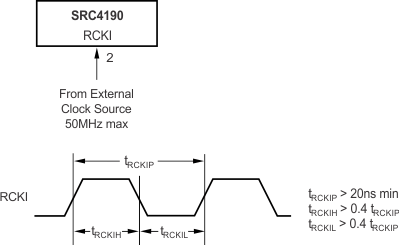 Figure 64. Reference Clock Input Connections and Timing Requirements
8.2.2.2 Interfacing to Digital Audio Receivers and Transmitters
The SRC4190 input and output ports are designed to interface to a variety of audio devices, including receivers and transmitters commonly used for AES/EBU, S/PDIF, and CP1201 communications. Texas Instruments manufactures the DIR1703 digital audio interface receiver and the DIT4096 and DIT4192 digital audio transmitters to address these applications.
Figure 65 illustrates interfacing the DIR1703 to the SRC4190 input port. The DIR1703 operates from a single 3.3‑V supply, which requires the VIO supply for the SRC4190 to be set to 3.3-V for interface compatibility.
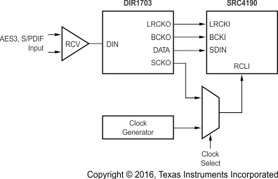 Figure 65. Interfacing the SRC4190 to the DIR1703 Digital Audio Interface Receiver
Figure 66 shows the interface between the SRC4190 output port and the DIT4096 or DIT4192 audio serial port. Once again, the VIO supplies for both the SRC4190, DIT4096, and DIT4192 are set to 3.3 V for compatibility.
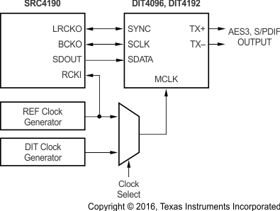 Figure 66. Interfacing the SRC4190 to the DIT4096 and DIT4192 Digital Audio Interface Transmitter
Like the SRC4190 output port, the DIT4096 and DIT4192 audio serial port may be configured as a master or slave. In cases where the SRC4190 output port is set to master mode, TI recommends using the reference clock source (RCKI) as the master clock source (MCLK) for the DIT4096 and DIT4192, to ensure that the transmitter is synchronized to the SRC4190 output port data.
8.2.2.3 TDM Applications
The SRC4190 supports a TDM output mode, which allows multiple devices to be daisy-chained together to create a serial frame. Each device occupies one sub-frame within a frame, and each sub-frame carries two channels (Left followed by Right). Each sub-frame is 64 bits long, with 32 bits allotted for each channel. The audio data for each channel is Left Justified within the allotted 32 bits. Figure 66 illustrates the TDM frame format, while Figure 68 shows the TDM input timing parameters, which are listed in Switching Characteristics.

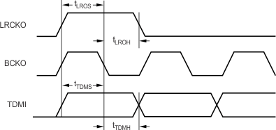 Figure 68. Input Timing for TDM Mode
The frame rate is equal to the output sampling frequency. The BCKO frequency for the TDM interface is
N × 64 fS, where N is the number of devices included in the daisy chain. For master mode, the output BCKO frequency is fixed to the reference clock (RCKI) input frequency. The number of devices that can be daisy-chained in TDM mode is dependent upon the output sampling frequency and the BCKO frequency, leading to the numerical relationship in Equation 1
where
- fBCKO = Output port bit clock (BCKO) (27.136-MHz maximum)
- fS = Output port sampling (LRCKO) frequency (212-kHz maximum)
This relationship holds true for both slave and master modes. Figure 69 and Figure 70 show typical connection schemes for the TDM mode. Although the TMS320C671x DSP family is shown as the audio processing engine in these figures, other TI digital signal processors with a multi-channel buffered serial port (McBSPTM) may also function with this arrangement. Interfacing to processors from other manufacturers is also possible. See Figure 62, along with the equivalent serial port timing diagrams shown in the DSP data sheet, to determine compatibility.
 Figure 69. TDM Interface With All Devices as Slaves
 Figure 70. TDM Interface With One Device as Master to Multiple Slaves
8.2.2.4 Pin Compatibility With the Analog Devices AD1895 and AD1896
The SRC4190 is pin and function-compatible with the AD1895 and AD1896 when observing the guidelines indicated in the following paragraphs.
8.2.2.4.1 Power Supplies
To ensure compatibility, the VDD_IO and VDD_CORE supplies of the AD1895 and AD1896 must be set to 3.3 V, while the VIO and VDD supplies of the SRC4190 must be set to 3.3 V.
8.2.2.4.2 Pin 1 Connection
For the AD1895, pin 1 is not connected. For the SRC4190, pin 1 (LGRP) functions as the low group delay selection input, and must not be left unconnected. LGRP must be connected to either digital ground or the VIO supply, dependent upon the desired group delay.
8.2.2.4.3 Crystal Oscillator
The SRC4190 does not have an on-chip crystal oscillator. An external reference clock is required at the RCKI pin.
8.2.2.4.4 Reference Clock Frequency
The reference clock input frequency for the SRC4190 must be no higher than 30 MHz, in order to match the master clock frequency specification of the AD1895 and AD1896. In addition, the SRC4190 does not support the 768-fS reference clock rate.
8.2.2.4.5 Master Mode Maximum Sampling Frequency
When the input or output ports are set to master mode, the maximum sampling frequency must be limited to
96 kHz in order to support the AD1895 and AD1896 specification. This is despite the fact that the SRC4190 supports a maximum sampling frequency of 212 kHz in master mode. The user must consider building an option into his or her design to support the higher sampling frequency of the SRC4190.
8.2.2.4.6 Matched Phase Mode
Due to the internal architecture of the SRC4190, it does not require or support the matched phase mode of the AD1896. Given multiple SRC4190 devices, if all reference clock (RCKI) inputs are driven from the same clock source, the devices is phase matched.
8.2.3 Application Curves
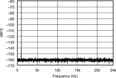 Figure 71. FFT With 1 kHz Input Tone at –60 dBFS
(44.1 kHz:48 kHz)
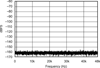 Figure 72. FFT With 1 kHz Input Tone at –60 dBFS
(44.1 kHz:96 kHz)