SBFS023C June   2003  – December 2016 SRC4190

PRODUCTION DATA.  

  1. Features
  2. Applications
  3. Description
  4. Revision History
  5. Pin Configuration and Functions
  6. Specifications
    1. 6.1 Absolute Maximum Ratings
    2. 6.2 ESD Ratings
    3. 6.3 Recommended Operating Conditions
    4. 6.4 Thermal Information
    5. 6.5 Electrical Characteristics
    6. 6.6 Switching Characteristics
    7. 6.7 Typical Characteristics
  7. Detailed Description
    1. 7.1 Overview
    2. 7.2 Functional Block Diagram
    3. 7.3 Feature Description
      1. 7.3.1 Soft Mute Function
      2. 7.3.2 Ready Output
    4. 7.4 Device Functional Modes
      1. 7.4.1 Bypass Mode
      2. 7.4.2 Audio Port Modes
      3. 7.4.3 Input Port Operation
      4. 7.4.4 Output Port Operation
  8. Application and Implementation
    1. 8.1 Application Information
    2. 8.2 Typical Application
      1. 8.2.1 Design Requirements
      2. 8.2.2 Detailed Design Procedure
        1. 8.2.2.1 Reference Clock
        2. 8.2.2.2 Interfacing to Digital Audio Receivers and Transmitters
        3. 8.2.2.3 TDM Applications
        4. 8.2.2.4 Pin Compatibility With the Analog Devices AD1895 and AD1896
          1. 8.2.2.4.1 Power Supplies
          2. 8.2.2.4.2 Pin 1 Connection
          3. 8.2.2.4.3 Crystal Oscillator
          4. 8.2.2.4.4 Reference Clock Frequency
          5. 8.2.2.4.5 Master Mode Maximum Sampling Frequency
          6. 8.2.2.4.6 Matched Phase Mode
      3. 8.2.3 Application Curves
  9. Power Supply Recommendations
  10. 10Layout
    1. 10.1 Layout Guidelines
      1. 10.1.1 Power Supply Pins
      2. 10.1.2 Digital Interface
    2. 10.2 Layout Example
  11. 11Device and Documentation Support
    1. 11.1 Documentation Support
      1. 11.1.1 Related Documentation
    2. 11.2 Receiving Notification of Documentation Updates
    3. 11.3 Community Resources
    4. 11.4 Trademarks
    5. 11.5 Electrostatic Discharge Caution
    6. 11.6 Glossary
  12. 12Mechanical, Packaging, and Orderable Information

Package Options

Mechanical Data (Package|Pins)
Thermal pad, mechanical data (Package|Pins)
Orderable Information

Layout

Layout Guidelines

Power Supply Pins

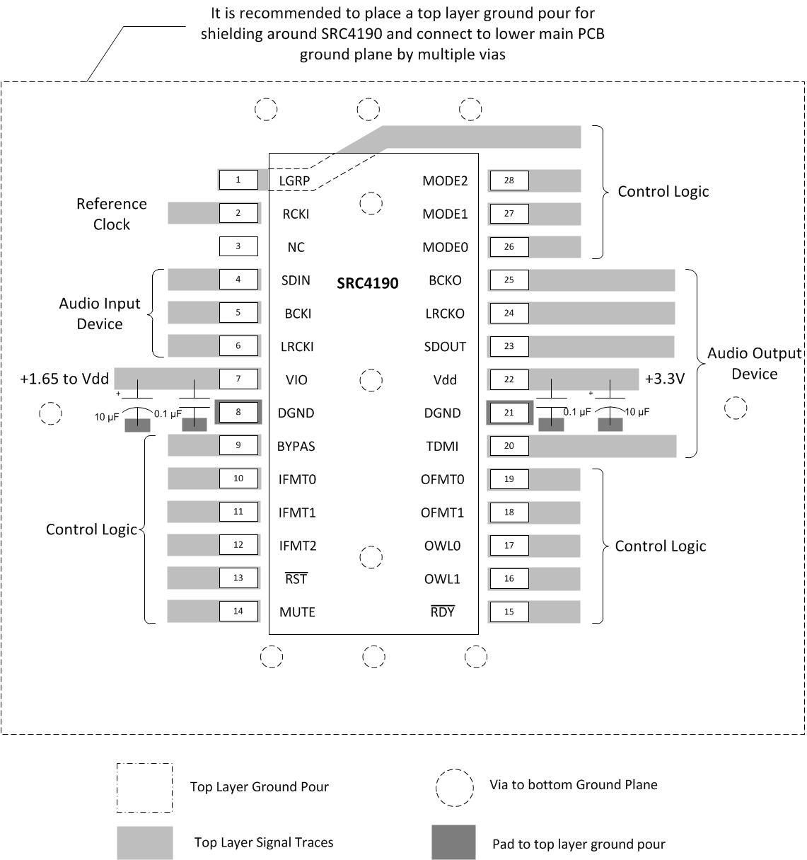
Place power supply decoupling capacitors as close to the supply pins as possible to minimize noise on device supplies. TI recommends values of 10 µF and 0.1 µF for these capacitors.

Digital Interface

With high frequency clocks being input or produced on the digital interface pins, reflections can become an issue, causing system noise. A series resistor in the tens of ohms can be placed on each trace to minimize reflections.

Layout Example

SRC4190 layout_sbfs023.gif Figure 73. Diagram of an Example Layout