SLES217D November   2010  – March 2015 TAS5630B

PRODUCTION DATA.  

  1. Features
  2. Applications
  3. Description
  4. Revision History
  5. Pin Configuration and Functions
  6. Specifications
    1. 6.1 Absolute Maximum Ratings
    2. 6.2 ESD Ratings
    3. 6.3 Recommended Operating Conditions
    4. 6.4 Thermal Information
    5. 6.5 Electrical Characteristics
    6. 6.6 Audio Characteristics (BTL)
    7. 6.7 Audio Specification (Single-Ended Output)
    8. 6.8 Audio Specification (PBTL)
    9. 6.9 Typical Characteristics
      1. 6.9.1 BTL Configuration
      2. 6.9.2 SE Configuration
      3. 6.9.3 PBTL Configuration
  7. Detailed Description
    1. 7.1 Overview
    2. 7.2 Functional Block Diagram
    3. 7.3 Feature Description
      1. 7.3.1  Power Supplies
      2. 7.3.2  System Power-Up and Power-Down Sequence
        1. 7.3.2.1 Powering Up
        2. 7.3.2.2 Powering Down
      3. 7.3.3  Error Reporting
      4. 7.3.4  Device Protection System
      5. 7.3.5  Pin-to-Pin Short-Circuit Protection (PPSC)
      6. 7.3.6  Overtemperature Protection
      7. 7.3.7  Undervoltage Protection (UVP) and Power-On Reset (POR)
      8. 7.3.8  Device Reset
      9. 7.3.9  Click and Pop in SE-Mode
      10. 7.3.10 PBTL Overload and Short Circuit
      11. 7.3.11 Oscillator
    4. 7.4 Device Functional Modes
  8. Application and Implementation
    1. 8.1 Application Information
      1. 8.1.1 PCB Material Recommendation
      2. 8.1.2 PVDD Capacitor Recommendation
      3. 8.1.3 Decoupling Capacitor Recommendations
      4. 8.1.4 System Design Considerations
    2. 8.2 Typical Application
      1. 8.2.1 Typical Application Schematic
        1. 8.2.1.1 Design Requirements
        2. 8.2.1.2 Detailed Design Procedure
        3. 8.2.1.3 Application Curves
      2. 8.2.2 Typical Differential-Input BTL Application With BD Modulation Filters
      3. 8.2.3 Typical Differential (2N) PBTL Application With BD Modulation Filters
      4. 8.2.4 Typical SE Application
      5. 8.2.5 Typical 2.1 System Differential-Input BTL and Unbalanced-Input SE Application
      6. 8.2.6 Typical Differential-Input BTL Application With BD Modulation Filters, DKD Package
  9. Power Supply Recommendations
  10. 10Layout
    1. 10.1 Layout Guidelines
    2. 10.2 Layout Example
  11. 11Device and Documentation Support
    1. 11.1 Trademarks
    2. 11.2 Electrostatic Discharge Caution
    3. 11.3 Glossary
  12. 12Mechanical, Packaging, and Orderable Information

Package Options

Mechanical Data (Package|Pins)
Thermal pad, mechanical data (Package|Pins)
Orderable Information

10 Layout

10.1 Layout Guidelines

Use an unbroken ground plane to have a good low-impedance and -inductance return path to the power supply for power and audio signals. PCB layout, audio performance and EMI are linked closely together. The circuit contains high, fast-switching currents; therefore, care must be taken to prevent damaging voltage spikes. Routing of the audio input should be kept short and together with the accompanying audio-source ground. A local ground area underneath the device is important to keep solid to minimize ground bounce. It is always good practice to follow the EVM layout as a guideline.

Netlist for this printed circuit board is generated from the schematic in Figure 18.

10.2 Layout Example
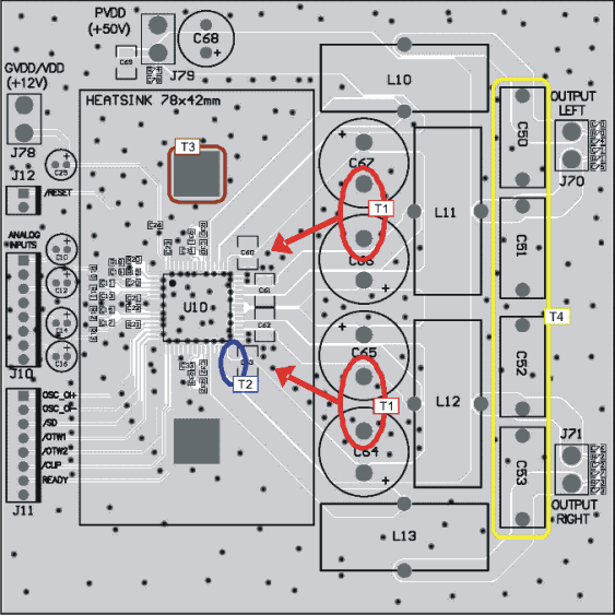
TAS5630B pcb_les220.gif
Note T1: PVDD bulk decoupling capacitors C60–C64 should be as close as possible to the PVDD_X and GND_X pins; the heat sink sets the distance. Wide traces should be routed on the top layer with direct connection to the pins and without going through vias. No vias or traces should be blocking the current path.
Note T2: Close decoupling of PVDD with low impedance X7R ceramic capacitors is placed under the heat sink and close to the pins. This is valid for C60, C61, C62, and C63.
Note T3: Heat sink must have a good connection to PCB ground.
Note T4: Output filter capacitors must be linear in the applied voltage range, preferably metal film types.
Figure 23. Printed Circuit Board – Top Layer
TAS5630B pcb_bot_les220.gif
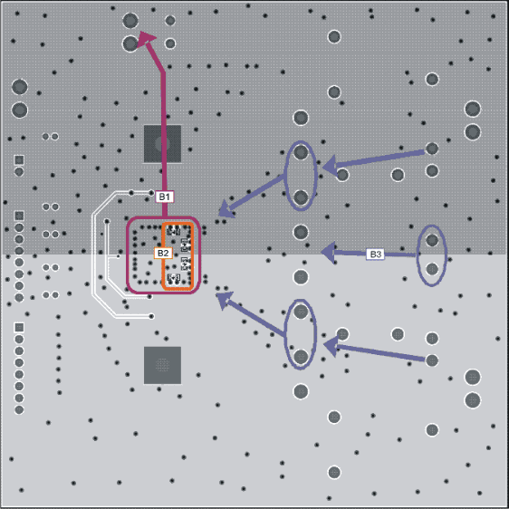
Note B1: It is important to have a direct-low impedance return path for high current back to the power supply. Keep impedance low from top to bottom side of PCB through a lot of ground vias.
Note B2: Bootstrap low-impedance X7R ceramic capacitors placed on bottom side provide a short, low-inductance current loop.
Note B3: Return currents from bulk capacitors and output filter capacitors
Figure 24. Printed Circuit Board – Bottom Layer