SLASE77A March 2016 – March 2016 TAS5733L
PRODUCTION DATA.
- 1 Features
- 2 Applications
- 3 Description
- 4 Revision History
- 5 Pin Configuration and Functions
-
6 Specifications
- 6.1 Absolute Maximum Ratings
- 6.2 ESD Ratings
- 6.3 Recommended Operating Conditions
- 6.4 Thermal Characteristics
- 6.5 Electrical Characteristics
- 6.6 Speaker Amplifier Characteristics
- 6.7 Protection Characteristics
- 6.8 Master Clock Characteristics
- 6.9 I²C Interface Timing Requirements
- 6.10 Serial Audio Port Timing Requirements
- 6.11 Typical Characteristics - Stereo BTL Mode
- 6.12 Typical Characteristics - Mono PBTL Mode
-
7 Detailed Description
- 7.1 Overview
- 7.2 Functional Block Diagram
- 7.3 Audio Signal Processing Overview
- 7.4 Feature Description
- 7.5 Device Functional Modes
- 7.6 Programming
- 7.7
Register Maps
- 7.7.1 Register Summary
- 7.7.2
Detailed Register Descriptions
- 7.7.2.1 Clock Control Register (0x00)
- 7.7.2.2 Device ID Register (0x01)
- 7.7.2.3 Error Status Register (0x02)
- 7.7.2.4 System Control Register 1 (0x03)
- 7.7.2.5 Serial Data Interface Register (0x04)
- 7.7.2.6 System Control Register 2 (0x05)
- 7.7.2.7 Soft Mute Register (0x06)
- 7.7.2.8 Volume Registers (0x07, 0x08, 0x09)
- 7.7.2.9 Volume Configuration Register (0x0E)
- 7.7.2.10 Modulation Limit Register (0x10)
- 7.7.2.11 Interchannel Delay Registers (0x11, 0x12, 0x13, and 0x14)
- 7.7.2.12 PWM Shutdown Group Register (0x19)
- 7.7.2.13 Start/Stop Period Register (0x1A)
- 7.7.2.14 Oscillator Trim Register (0x1B)
- 7.7.2.15 BKND_ERR Register (0x1C)
- 7.7.2.16 Input Multiplexer Register (0x20)
- 7.7.2.17 PWM Output MUX Register (0x25)
- 7.7.2.18 AGL Control Register (0x46)
- 7.7.2.19 PWM Switching Rate Control Register (0x4F)
- 7.7.2.20 Bank Switch and EQ Control (0x50)
-
8 Application and Implementation
- 8.1 Application Information
- 8.2
Typical Applications
- 8.2.1
Stereo Bridge Tied Load Application
- 8.2.1.1 Design Requirements
- 8.2.1.2 Detailed Design Procedure
- 8.2.1.3 Application Performance Plots
- 8.2.2 Mono Parallel Bridge Tied Load Application
- 8.2.1
Stereo Bridge Tied Load Application
- 9 Power Supply Recommendations
- 10Layout
- 11Device and Documentation Support
- 12Mechanical, Packaging, and Orderable Information
Package Options
Mechanical Data (Package|Pins)
- DCA|48
Thermal pad, mechanical data (Package|Pins)
- DCA|48
Orderable Information
6 Specifications
6.1 Absolute Maximum Ratings
over operating free-air temperature range (unless otherwise noted)(1)| VALUE | UNIT | ||
|---|---|---|---|
| Supply voltage | DVDD, AVDD | –0.3 to 3.6 | V |
| PVDD | –0.3 to 20 | ||
| Input voltage | 3.3-V digital input | –0.5 to DVDD + 0.5 | V |
| 5-V tolerant(2) digital input (except MCLK) | –0.5 to DVDD + 2.5(4) | ||
| 5-V tolerant MCLK input | –0.5 to AVDD + 2.5(4) | ||
| AMP_OUT_x to GND | 22(3) | V | |
| BSTRP_x to GND | 29(3) | V | |
| Operating free-air temperature | 0 to 85 | °C | |
| Storage temperature range, Tstg | –40 to 125 | °C | |
(1) Stresses beyond those listed under Absolute Maximum Ratings may cause permanent damage to the device. These are stress ratings only and functional operation of the device at these or any other conditions beyond those indicated under Recommended Operating Conditions is not implied. Exposure to absolute-maximum conditions for extended periods may affect device reliability.
(2) 5-V tolerant inputs are PDN, RST, SCLK, LRCK, MCLK, SDIN, SDA, and SCL.
(3) DC voltage + peak ac waveform measured at the pin should be below the allowed limit for all conditions.
(4) Maximum pin voltage should not exceed 6 V.
6.2 ESD Ratings
| VALUE | UNIT | |||
|---|---|---|---|---|
| V(ESD) | Electrostatic discharge | Human-body model (HBM), per ANSI/ESDA/JEDEC JS-001(1) | ±4000 | V |
| Charged-device model (CDM), per JEDEC specification JESD22-C101(2) | ±1500 | |||
(1) JEDEC document JEP155 states that 500-V HBM allows safe manufacturing with a standard ESD control process.
(2) JEDEC document JEP157 states that 250-V CDM allows safe manufacturing with a standard ESD control process.
6.3 Recommended Operating Conditions
| MIN | NOM | MAX | UNIT | |||
|---|---|---|---|---|---|---|
| DVDD, AVDD | Digital, analog supply voltage | 3 | 3.3 | 3.6 | V | |
| PVDD | Output power devices supply voltage | 8 | 16.5(1)(2) | V | ||
| VIH | High-level input voltage | 5-V tolerant | 2 | V | ||
| VIL | Low-level input voltage | 5-V tolerant | 0.8 | V | ||
| TA | Operating ambient temperature range | 0 | 85 | °C | ||
| TJ (2) | Operating junction temperature range | 0 | 125 | °C | ||
| RL | Load impedance | 4 | 8 | Ω | ||
| RL | Load impedance in PBTL | 2 | Ω | |||
| LO | Output-filter inductance | Minimum output inductance under short-circuit condition | 10 | μH | ||
(1) For operation at PVDD levels greater than 14.5 V, the modulation limit must be set to 96.1% or lower via the control port register 0x10.
(2) 16.5 V is the maximum recommended voltage for continuous operation of the TAS5733L device. Testing and characterization of the device is performed up to and including 16.5 V to ensure “in system” design margin. However, continuous operation at these levels is not recommended. Operation above the maximum recommended voltage may result in reduced performance, errant operation, and reduction in device reliability.
6.4 Thermal Characteristics
| THERMAL METRIC(1) | DCA (48 PINS) | UNITS | ||||
|---|---|---|---|---|---|---|
| Special Test Case | JEDEC Standard 2-Layer PCB | JEDEC Standard 4-Layer PCB | TAS5733LEVM | |||
| θJA | Junction-to-ambient thermal resistance(2) | 50.7 | 27.6 | 25.0 | °C/W | |
| θJCtop | Junction-to-case (top) thermal resistance(3) | 14.9 | 16.7 | °C/W | ||
| θJB | Junction-to-board thermal resistance(4) | 6.9 | 7.9 | °C/W | ||
| ψJT | Junction-to-top characterization parameter(5) | 1.2 | 0.8 | 0.7 | °C/W | |
| ψJB | Junction-to-board characterization parameter(6) | 11.8 | 7.8 | 5.8 | °C/W | |
| θJCbot | Junction-to-case (bottom) thermal resistance(7) | 1.7 | 2.2 | °C/W | ||
(1) For more information about traditional and new thermal metrics, see the Semiconductor and IC Package Thermal Metrics application report (SPRA953).
(2) The junction-to-ambient thermal resistance under natural convection is obtained in a simulation on a JEDEC-standard, high-K board, as specified in JESD51-7, in an environment described in JESD51-2a.
(3) The junction-to-case (top) thermal resistance is obtained by simulating a cold plate test on the package top. No specific JEDEC-standard test exists, but a close description can be found in the ANSI SEMI standard G30-88.
(4) The junction-to-board thermal resistance is obtained by simulating in an environment with a ring cold plate fixture to control the PCB temperature, as described in JESD51-8.
(5) The junction-to-top characterization parameter, ψJT, estimates the junction temperature of a device in a real system and is extracted from the simulation data for obtaining RθJA, using a procedure described in JESD51-2a (sections 6 and 7).
(6) The junction-to-board characterization parameter, ψJB, estimates the junction temperature of a device in a real system and is extracted from the simulation data for obtaining RθJA, using a procedure described in JESD51-2a (sections 6 and 7).
(7) The junction-to-case (bottom) thermal resistance is obtained by simulating a cold plate test on the exposed (power) pad. No specific JEDEC standard test exists, but a close description can be found in the ANSI SEMI standard G30-88.
Spacer
Spacer
6.5 Electrical Characteristics
TA = 25°, PVDD_x = 12 V, DVDD = AVDD = 3.3 V, RL= 8 Ω, BTL BD mode, fS = 48 kHz (unless otherwise noted)| PARAMETER | TEST CONDITIONS | MIN | TYP | MAX | UNIT | ||
|---|---|---|---|---|---|---|---|
| VOH | High-level output voltage | ADR/FAULT and SDA | IOH = –4 mA DVDD = AVDD = 3 V |
2.4 | V | ||
| VOL | Low-level output voltage | IOL = 4 mA DVDD = AVDD = 3 V |
0.5 | V | |||
| IIL | Low-level input current | Digital Inputs | VI < VIL
DVDD = AVDD = 3.6 V |
75 | μA | ||
| IIH | High-level input current | VI > VIH
DVDD = AVDD = 3.6 V |
75 | μA | |||
| IDD | 3.3-V supply current | 3.3-V supply voltage (DVDD, AVDD) |
Normal mode | 49 | 68 | mA | |
| Reset (RST = low, PDN = high) | 23 | 38 | |||||
6.6 Speaker Amplifier Characteristics
PVDD = 12 V, BTL BD mode, AVDD = DVDD = 3.3 V, fS = 48 KHz, RL = 8 Ω, audio frequency = 1 kHz, AES17 filter, fPWM = 384 kHz, TA = 25°C (unless otherwise specified). All performance is in accordance with recommended operating conditions and as tested on the TAS5733L EVM.| PARAMETER | TEST CONDITIONS | MIN | TYP | MAX | UNIT | ||
|---|---|---|---|---|---|---|---|
| PO | Power output per channel | PVDD = 12 V, 10% THD, 1-kHz input signal | 10 | W | |||
| PVDD = 12 V, 7% THD, 1-kHz input signal | 9 | ||||||
| PVDD = 12 V, 1% THD, 1-kHz input signal | 7.5 | ||||||
| PVDD = 13.2 V, 10% THD, 1-kHz input signal | 12 | ||||||
| PVDD = 13.2 V, 7% THD, 1-kHz input signal | 11 | ||||||
| PVDD = 13.2 V, 1% THD, 1-kHz input signal | 9 | ||||||
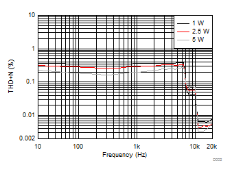
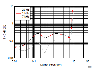
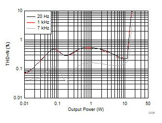
| THD+N | Total harmonic distortion + noise | PVDD = 12 V, PO = 1 W | 0.25 | % | |||
| PVDD = 13.2 V, PO = 1 W | 0.3 | ||||||
| Vn | Output integrated noise (rms) | A-weighted | 30 | μV | |||
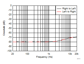
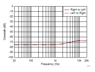
| Crosstalk | PO = 1 W, f = 1 kHz (BD Mode), PVDD = 12 V | –79 | dB | ||||
| PO =1 W, f = 1 kHz (AD Mode), PVDD = 12 V | –62 | dB | |||||
| Output switching frequency | 11.025, 22.05, 44.1-kHz data rate ±2% | 288 | kHz | ||||
| 48, 24, 12, 8, 16, 32-kHz data rate ±2% | 384 | ||||||
| IPVDD | Supply current | No load (PVDD) | Normal mode | 16 | 25 | mA | |
| Reset (RST = low, PDN = high) | 3 | 8 | |||||
| rDS(on)(1) | Drain-to-source resistance, low side | TJ = 25°C, includes metallization resistance | 120 | mΩ | |||
| Drain-to-source resistance, high side | TJ = 25°C, includes metallization resistance | 120 | |||||
| RPD | Internal pulldown resistor at the output of each half-bridge | Connected when drivers are in the high-impedance state to provide bootstrap capacitor charge. | 3 | kΩ | |||
(1) This does not include bond-wire or pin resistance.
6.7 Protection Characteristics
TA = 25°, PVDD_x = 12 V, DVDD = AVDD = 3.3 V, RL= 8 Ω, BTL BD mode, fS = 48 kHz (unless otherwise noted)| PARAMETER | TEST CONDITIONS | MIN | TYP | MAX | UNIT | ||
|---|---|---|---|---|---|---|---|
| Vuvp(fall) | Undervoltage protection limit | PVDD falling | 5.4 | V | |||
| Vuvp(rise) | Undervoltage protection limit | PVDD rising | 5.8 | V | |||
| OTE | Overtemperature error | 150 | °C | ||||
| IOC | Overcurrent limit protection | 4 | A | ||||
| IOCT | Overcurrent response time | 150 | ns | ||||
6.8 Master Clock Characteristics(1)
PVDD = 12 V, BTL BD mode, AVDD = DVDD = 3.3 V, fS = 48 kHz, RL = 8 Ω, audio frequency = 1 kHz, AES17 filter, fPWM = 384 kHz, TA = 25°C (unless otherwise specified). All performance is in accordance with recommended operating conditions (unless otherwise specified).| PARAMETER | TEST CONDITIONS | MIN | TYP | MAX | UNIT | |
|---|---|---|---|---|---|---|
| PLL INPUT PARAMETERS | ||||||
| fMCLKI | MCLK frequency | 2.8224 | 24.576 | MHz | ||
| MCLK duty cycle | 40% | 50% | 60% | |||
| tr / tf(MCLK) | Rise/fall time for MCLK | 5 | ns | |||
(1) For clocks related to the serial audio port, please see Serial Audio Port Timing Requirements.
6.9 I²C Interface Timing Requirements
| MIN | NOM | MAX | UNIT | ||
|---|---|---|---|---|---|
| tw(RST) | Pulse duration, RST active | 100 | μs | ||
| td(I²C_ready) | Time to enable I²C after RST goes high | 13.5 | ms | ||
| fSCL | Frequency, SCL | 400 | kHz | ||
| tw(H) | Pulse duration, SCL high | 0.6 | μs | ||
| tw(L) | Pulse duration, SCL low | 1.3 | μs | ||
| tr | Rise time, SCL and SDA | 300 | ns | ||
| tf | Fall time, SCL and SDA | 300 | ns | ||
| tsu1 | Setup time, SDA to SCL | 100 | ns | ||
| th1 | Hold time, SCL to SDA | 0 | ns | ||
| t(buf) | Bus free time between stop and start conditions | 1.3 | μs | ||
| tsu2 | Setup time, SCL to start condition | 0.6 | μs | ||
| th2 | Hold time, start condition to SCL | 0.6 | μs | ||
| tsu3 | Setup time, SCL to stop condition | 0.6 | μs | ||
| CL | Load capacitance for each bus line | 400 | pF | ||
6.10 Serial Audio Port Timing Requirements
over recommended operating conditions (unless otherwise noted)| PARAMETER | TEST CONDITIONS | MIN | TYP | MAX | UNIT | |
|---|---|---|---|---|---|---|
| fSCLKIN | Frequency, SCLK 32 × fS, 48 × fS, 64 × fS | CL ≤ 30 pF | 1.024 | 12.288 | MHz | |
| tsu1 | Setup time, LRCK to SCLK rising edge | 10 | ns | |||
| th1 | Hold time, LRCK from SCLK rising edge | 10 | ns | |||
| tsu2 | Setup time, SDIN to SCLK rising edge | 10 | ns | |||
| th2 | Hold time, SDIN from SCLK rising edge | 10 | ns | |||
| LRCK frequency | 8 | 48 | 48 | kHz | ||
| SCLK duty cycle | 40% | 50% | 60% | |||
| LRCK duty cycle | 40% | 50% | 60% | |||
| SCLK rising edges between LRCK rising edges | 32 | 64 | SCLK edges | |||
| t(edge) | LRCK clock edge with respect to the falling edge of SCLK | –1/4 | 1/4 | SCLK period | ||
| tr/tf | Rise/fall time for SCLK/LRCK | 8 | ns | |||
| LRCK allowable drift before LRCK reset | 4 | MCLKs | ||||
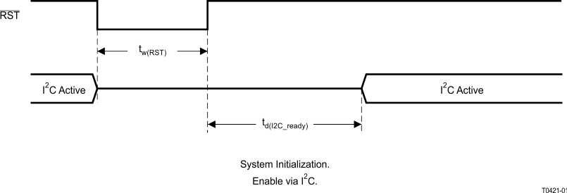
NOTE:
On power up, hold the TAS5733L RST LOW for at least 100 μs after DVDD has reached 3 V.NOTE:
If RST is asserted LOW while PDN is LOW, then RST must continue to be held LOW for at least 100 μs after PDN is deasserted (HIGH). Figure 2. SCL and SDA Timing
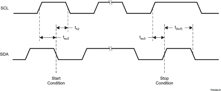 Figure 3. Start and Stop Conditions Timing
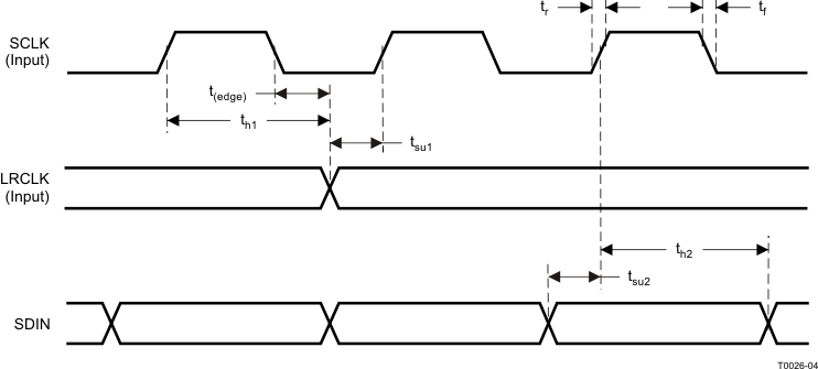 Figure 4. Serial Audio Port Timing
6.11 Typical Characteristics - Stereo BTL Mode
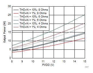
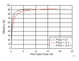
| RL = 8 Ω | ||
| Total Output Power includes power delivered from both amplifier outputs. For instance, 40 W of total output power means 2 × 20 W, with 20 W delivered by one channel and 20 W delivered by the other channel. | ||
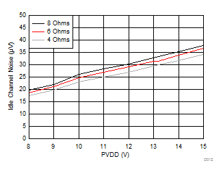
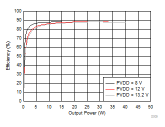
| RL = 4 Ω | ||
| Total Output Power includes power delivered from both amplifier outputs. For instance, 40 W of total output power means 2 × 20 W, with 20 W delivered by one channel and 20 W delivered by the other channel. | ||
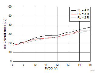
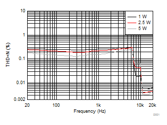
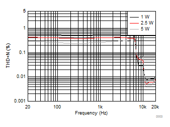
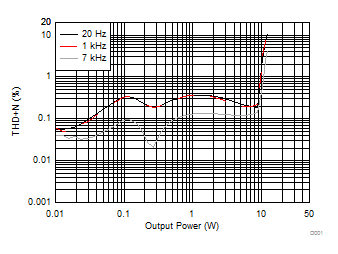
6.12 Typical Characteristics - Mono PBTL Mode
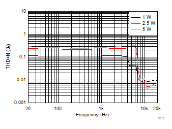
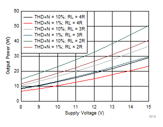
| PVDD = 12 V | RL = 4 Ω |
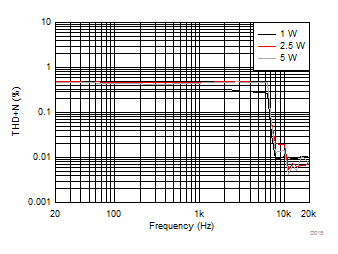
| PVDD = 12 V | RL = 2 Ω |
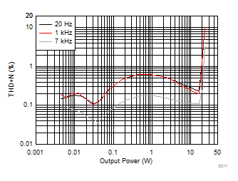
| PVDD = 12 V | RL = 3 Ω |
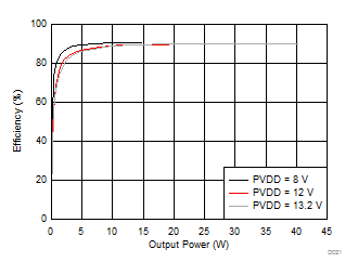
| RL = 2 Ω | ||
| Total Output Power includes power delivered from both amplifier outputs. For instance, 40 W of total output power means 2 × 20 W, with 20 W delivered by one channel and 20 W delivered by the other channel. | ||
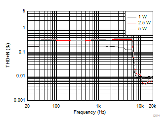
| PVDD = 12 V | RL = 3 Ω |
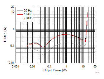
| PVDD = 12 V | RL = 4 Ω |
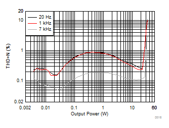
| PVDD = 12 V | RL = 2 Ω |
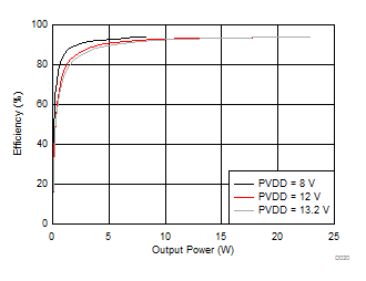
| RL = 4 Ω | ||
| Total Output Power includes power delivered from both amplifier outputs. For instance, 40 W of total output power means 2 × 20 W, with 20 W delivered by one channel and 20 W delivered by the other channel. | ||
