SLASEH7H October 2019 – January 2023 TAS5825M
PRODUCTION DATA
- 1 Features
- 2 Applications
- 3 Description
- 4 Revision History
- 5 Device Comparison Table
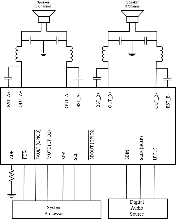
- 6 Pin Configuration and Functions
- 7 Specifications
- 8 Parameter Measurement Information
-
9 Detailed Description
- 9.1 Overview
- 9.2 Functional Block Diagram
- 9.3 Feature Description
- 9.4 Device Functional Modes
- 9.5 Programming and Control
- 9.6 Register Maps
-
10Application and Implementation
- 10.1 Application Information
- 10.2 Typical Applications
- 10.3 Power Supply Recommendations
- 10.4 Layout
- 11Device and Documentation Support
- 12Mechanical, Packaging, and Orderable Information
Package Options
Mechanical Data (Package|Pins)
- RHB|32
Thermal pad, mechanical data (Package|Pins)
- RHB|32
Orderable Information
3 Description
The TAS5825M is a stereo high-performance closed-loop Class-D with an integrated audio processor and up to 192-kHz support.
The powerful audio DSP core supports several advanced audio process flows such as 2×15 BQs, 3-Band DRC, Full-band AGL (Automatic Gain Limiter), Smart Amplifier Algorithm (Thermal and Excursion Protection), Bass enhancement, Spatializer, THD manager, PVDD Tracking, and Thermal Foldback. The TAS5825M has a 48-kHz or 96-kHz architecture with an integrated SRC (Sample Rate Convertor) that detects the input sample rate and auto-converts the input sample to the DSP target sample rate to avoid audio artifacts.
| PART NUMBER | PACKAGE(1) | BODY SIZE (NOM) |
|---|---|---|
| TAS5825M | VQFN (32) RHB | 5.00 mm × 5.00 mm |