SLASET9A May   2019  – January 2023 TAS5825P

PRODUCTION DATA  

  1. Features
  2. Applications
  3. Description
  4. Revision History
  5. Device Comparison Table
  6. Pin Configuration and Functions
  7. Specifications
    1. 7.1 Absolute Maximum Ratings
    2. 7.2 ESD Ratings
    3. 7.3 Recommended Operating Conditions
    4. 7.4 Thermal Information
    5. 7.5 Electrical Characteristics
    6. 7.6 Timing Requirements
    7. 7.7 Typical Characteristics
      1. 7.7.1 Bridge Tied Load (BTL) Configuration Curves with Hybrid Modulation
      2. 7.7.2 Parallel Bridge Tied Load (PBTL) Configuration With Hybrid Modulation
      3. 7.7.3 Bridge Tied Load (BTL) Configuration Curves with BD Modulation
      4. 7.7.4 Parallel Bridge Tied Load (PBTL) Configuration With BD Modulation
  8. Parameter Measurement Information
  9. Detailed Description
    1. 9.1 Overview
    2. 9.2 Functional Block Diagram
    3. 9.3 Feature Description
      1. 9.3.1 Power Supplies
      2. 9.3.2 Device Clocking
      3. 9.3.3 Serial Audio Port – Clock Rates
      4. 9.3.4 Clock Halt Auto-Recovery
      5. 9.3.5 Sample Rate on the Fly Change
      6. 9.3.6 Serial Audio Port - Data Formats and Bit Depths
      7. 9.3.7 Digital Audio Processing
      8. 9.3.8 Class-D Audio Amplifier
        1. 9.3.8.1 Speaker Amplifier Gain Select
        2. 9.3.8.2 Class D Loop Bandwidth and Switching Frequency Setting
    4. 9.4 Device Functional Modes
      1. 9.4.1 Software Control
      2. 9.4.2 Speaker Amplifier Operating Modes
        1. 9.4.2.1 BTL Mode
        2. 9.4.2.2 PBTL Mode
      3. 9.4.3 Low EMI Modes
        1. 9.4.3.1 Spread Spectrum
        2. 9.4.3.2 Channel to Channel Phase Shift
        3. 9.4.3.3 Multi-Devices PWM Phase Synchronization
          1. 9.4.3.3.1 Phase Synchronization With I2S Clock In Startup Phase
          2. 9.4.3.3.2 Phase Synchronization With GPIO
      4. 9.4.4 Thermal Foldback
      5. 9.4.5 Device State Control
      6. 9.4.6 Device Modulation
        1. 9.4.6.1 BD Modulation
        2. 9.4.6.2 1SPW Modulation
        3. 9.4.6.3 Hybrid Modulation
    5. 9.5 Programming and Control
      1. 9.5.1 I2 C Serial Communication Bus
      2. 9.5.2 I2 C Peripheral Address
        1. 9.5.2.1 Random Write
        2. 9.5.2.2 Sequential Write
        3. 9.5.2.3 Random Read
        4. 9.5.2.4 Sequential Read
        5. 9.5.2.5 DSP Memory Book, Page and BQ update
        6. 9.5.2.6 Checksum
          1. 9.5.2.6.1 Cyclic Redundancy Check (CRC) Checksum
          2. 9.5.2.6.2 Exclusive or (XOR) Checksum
      3. 9.5.3 Control via Software
        1. 9.5.3.1 Startup Procedures
        2. 9.5.3.2 Shutdown Procedures
        3. 9.5.3.3 Protection and Monitoring
          1. 9.5.3.3.1 Overcurrent Limit (Cycle-By-Cycle)
          2. 9.5.3.3.2 Overcurrent Shutdown (OCSD)
          3. 9.5.3.3.3 DC Detect
    6. 9.6 Register Maps
      1. 9.6.1 CONTROL PORT Registers
  10. 10Application and Implementation
    1. 10.1 Application Information
      1. 10.1.1 Bootstrap Capacitors
      2. 10.1.2 Inductor Selections
      3. 10.1.3 Power Supply Decoupling
      4. 10.1.4 Output EMI Filtering
    2. 10.2 Typical Applications
      1. 10.2.1 2.0 (Stereo BTL) System
      2. 10.2.2 79
      3. 10.2.3 Design Requirements
      4. 10.2.4 Detailed Design procedures
        1. 10.2.4.1 Step One: Hardware Integration
        2. 10.2.4.2 Step Two: Hardware Integration
        3. 10.2.4.3 Step Three: Software Integration
      5. 10.2.5 Application Curves
      6. 10.2.6 MONO (PBTL) Systems
      7. 10.2.7 Application Curves
    3. 10.3 Power Supply Recommendations
      1. 10.3.1 DVDD Supply
      2. 10.3.2 PVDD Supply
    4. 10.4 Layout
      1. 10.4.1 Layout Guidelines
        1. 10.4.1.1 General Guidelines for Audio Amplifiers
        2. 10.4.1.2 Importance of PVDD Bypass Capacitor Placement on PVDD Network
        3. 10.4.1.3 Optimizing Thermal Performance
          1. 10.4.1.3.1 Device, Copper, and Component Layout
          2. 10.4.1.3.2 Stencil Pattern
            1. 10.4.1.3.2.1 PCB footprint and Via Arrangement
            2. 10.4.1.3.2.2 Solder Stencil
      2. 10.4.2 Layout Example
  11. 11Device and Documentation Support
    1. 11.1 Device Support
      1. 11.1.1 Device Nomenclature
      2. 11.1.2 Development Support
    2. 11.2 Receiving Notification of Documentation Updates
    3. 11.3 Support Resources
    4. 11.4 Trademarks
    5. 11.5 Electrostatic Discharge Caution
    6. 11.6 Glossary
  12. 12Mechanical, Packaging, and Orderable Information

Package Options

Mechanical Data (Package|Pins)
Thermal pad, mechanical data (Package|Pins)
Orderable Information

Description

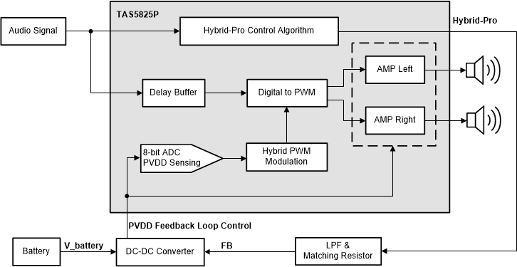
TAS5825P is a stereo high-efficiency Closed-Loop audio Class-D audio amplifier with an advanced Hybrid-Pro algorithm to improve system efficiency and reduce heat without clipping distortion.

The supply voltage (PVDD) of an audio amplifier is normally provided by a DC-DC converter. Compared with a fixed PVDD, a variable PVDD that fluctuates based on the audio signal significantly improves efficiency, lowers idle current, and reduces heat.

The powerful audio DSP core of TAS5825P implements a proprietary algorithm called Hybrid-Pro. The Hybrid-Pro algorithm detects the upcoming audio power demand and provides a PWM control signal for the former DC-DC converter via the Hybrid-Pro feedback pin (HPFB). The TAS5825P supports up to 4 ms of delay buffer to look ahead at the audio signal and prevent audio clipping distortion. In various experiments, the TAS5825P increased the runtime of 1S and 2S batteries by greater than 50% while continuously playing music.

Device Information(1)
PART NUMBERPACKAGEBODY SIZE (NOM)
TAS5825PVQFN (32) RHB5.00 mm × 5.00 mm
For all available packages, see the orderable addendum at the end of the data sheet.
GUID-A1A7D99F-8D5B-4AA7-AB10-720D6E772796-low.gif