SCPS253C January 2014 – September 2019 TCA5013
PRODUCTION DATA.
- 1 Features
- 2 Applications
- 3 Description
- 4 Revision History
- 5 Pin Configuration and Functions
-
6 Specifications
- 6.1 Absolute Maximum Ratings
- 6.2 Handling Ratings
- 6.3 Recommended Operating Conditions
- 6.4 Thermal Information
- 6.5 Electrical Characteristics—Power Supply and ESD
- 6.6 Electrical Characteristics—Card VCC
- 6.7 Electrical Characteristics—Card RST
- 6.8 Electrical Characteristics—Card CLK
- 6.9 Electrical Characteristics—Card Interface IO, C4 and C8
- 6.10 Electrical Characteristics—PRES
- 6.11 Electrical Characteristics—IOMC1 and IOMC2
- 6.12 Electrical Characteristics—CLKIN1 and CLKIN2
- 6.13 Electrical Characteristics—A0 and SHDN
- 6.14 Electrical Characteristics—INT
- 6.15 Electrical Characteristics—GPIO
- 6.16 Electrical Characteristics—SDA and SCL
- 6.17 Electrical Characteristics—Fault Condition Detection
- 6.18 I2C Interface Timing Requirements
- 6.19 I2C Interface Timing Characteristics
- 6.20 Synchronous Type 1 Card Activation Timing Characteristics
- 6.21 Synchronous Type 2 Card Activation Timing Characteristics
- 6.22 Card Deactivation Timing Characteristics
- 6.23 Typical Characteristics
- 7 Parameter Measurement Information
-
8 Detailed Description
- 8.1 Overview
- 8.2 Functional Block Diagram
- 8.3 Feature Description
- 8.4 Device Functional Modes
- 8.5 Programming
- 8.6 Register Maps
- 9 Application and Implementation
- 10Power Supply Recommendations
- 11Layout
- 12Device and Documentation Support
- 13Mechanical, Packaging, and Orderable Information
Package Options
Mechanical Data (Package|Pins)
- ZAH|48
Thermal pad, mechanical data (Package|Pins)
Orderable Information
8.4.4.7 Deactivation Sequence
After a card interface has been activated in a certain operating mode, it can be deactivated by I2C command or certain interrupt events (see Interrupt Operation). The deactivation sequence is the same regardless of what operating mode the card interface is in.
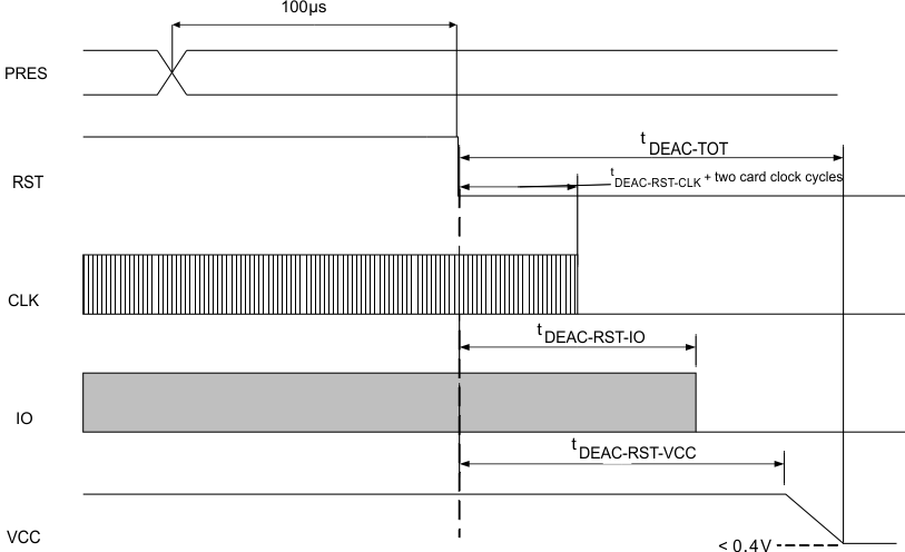
Figure 7 shows the deactivation sequence initiated by card extraction on the user card interface. It is to be noted that the deactivation sequence starts 100 µs after the transition on PRES. This delay is intended to provide a debounce period that provides unintended deactivation due to any glitch on the PRES pin. As mentioned previously any of the card interfaces may be deactivated due to a supervisor fault, over current fault or over temperature fault. In these cases there is no debounce period and the deactivation sequence is initiated as soon as the internal fault signal is asserted.
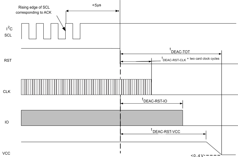
Figure 8 shows the deactivation of any card interface initiated by I2C command. If the card interface is activated in asynchronous mode, it can be deactivated by clearing (writing ‘0’) the START_ASYNC bit in the card interface settings register. To deactivate the user card interface when it is activated in synchronous mode, the START_SYNC bit should be cleared (write ‘0’).
 Figure 7. Deactivation Sequence
  Figure 8. Card Deactivation Sequence Initiated by I2C Command
 Table 4. Card Deactivation Timing Characteristics
| MIN | TYP | MAX | UNIT | |
|---|---|---|---|---|
| tDEAC-TOT | 0.4 | 0.5 | 0.6 | ms |
| tDEAC-RST-CLK | 10 | 12 | 15 | µs |
| tDEAC-RST-IO | 22 | 24 | 26 | µs |
| tDEAC-RST-VCC | 33 | 36 | 39 | µs |