SCPS164D MAY 2007 – February 2017 TCA6507
PRODUCTION DATA.
- 1 Features
- 2 Applications
- 3 Description
- 4 Revision History
- 5 Pin Configuration and Functions
- 6 Specifications
- 7 Parameter Measurement Information
-
8 Detailed Description
- 8.1 Overview
- 8.2 Functional Block Diagram
- 8.3 Feature Description
- 8.4 Device Functional Modes
- 8.5 Programming
- 8.6
Register Maps
- 8.6.1 Registers 0x00 - 0x02 (Select Registers)
- 8.6.2 Register 0x03 (Fade-ON Time)
- 8.6.3 Register 0x04 (Fully-ON Time)
- 8.6.4 Register 0x05 (Fade-OFF Time)
- 8.6.5 Register 0x06 - 0x07 (Fully-OFF Time)
- 8.6.6 Register 0x08 (Maximum Intensity per Bank)
- 8.6.7 Register 0x09 (One-Shot / Master Intensity)
- 8.6.8 Register 0x0A (Initialization Register)
- 9 Application and Implementation
- 10Power Supply Recommendations
- 11Layout
- 12Device and Documentation Support
- 13Mechanical, Packaging, and Orderable Information
Package Options
Mechanical Data (Package|Pins)
Thermal pad, mechanical data (Package|Pins)
- RUE|12
Orderable Information
9 Application and Implementation
NOTE
Information in the following applications sections is not part of the TI component specification, and TI does not warrant its accuracy or completeness. TI’s customers are responsible for determining suitability of components for their purposes. Customers must validate and test their design implementation to confirm system functionality.
9.1 Application Information
Applications of the TCA6507 contains an I2C (or SMBus) master device. The TCA6507 is used to control the blinking pattern of LEDs or as a general purpose output.
9.2 Typical Application
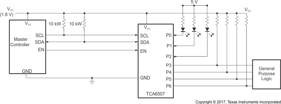
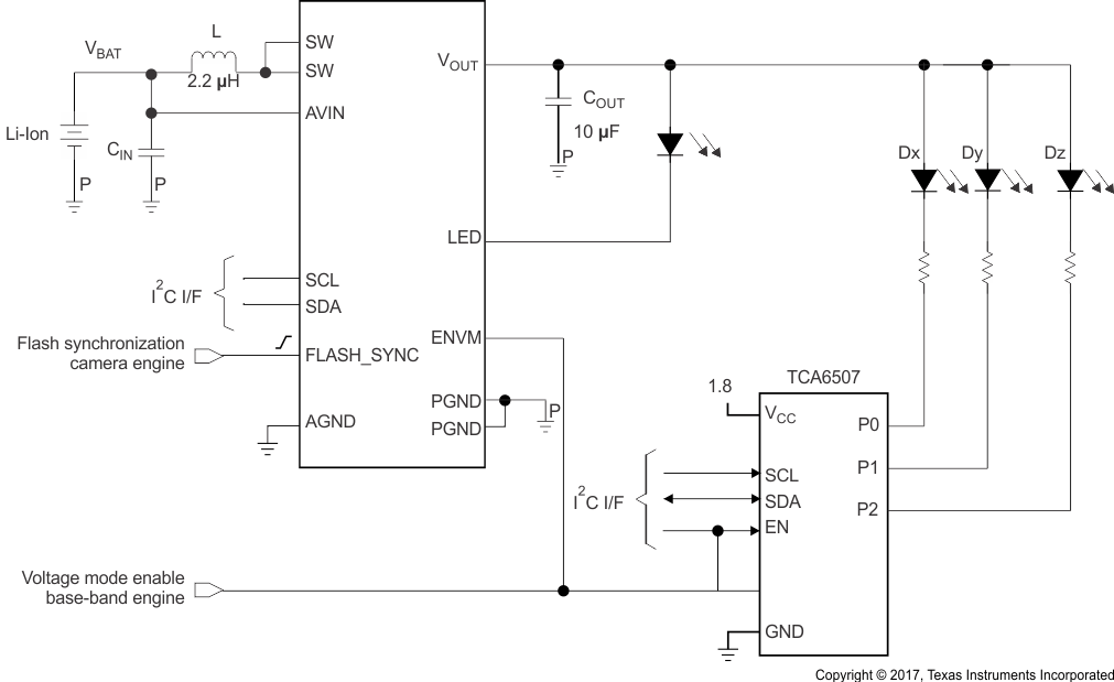
Figure 23 shows a general application in which the TCA6507 can be used. Each LED output is driving one LED. Figure 26 highlights another application where the TPS61052 boost converter and high-power LED driver and TCA6507 7-bit LED driver can be used in combination for applications requiring flashlight functionality and/or high-brightness indicator/backlight LEDs.
 Figure 23. Typical Application
9.2.1 Design Requirements
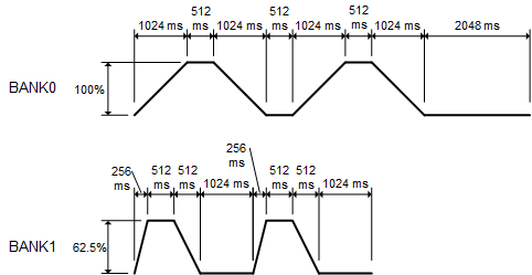
For the typical application example, the TCA6507 is set up to blink the P0 with Bank0 pattern, P1 fully on, and P2 with Bank1 blinking pattern. The banks is setup to the flashing pattern defined in Figure 24. The options for lengths of time for each section can be seen in Table 7.
 Figure 24. Blinking Pattern for the Two Banks
9.2.2 Detailed Design Procedure
For the typical application blinking pattern seen in Figure 24, the desired values are listed in Table 23, with the corresponding registers and values.
Table 23. LED Pattern
| SECTION | BANK1 VALUE | BANK0 VALUE | UNIT | REGISTER | BANK1 NIBBLE (HEX) | BANK0 NIBBLE (HEX) | REGISTER VALUE (HEX) |
|---|---|---|---|---|---|---|---|
| Fade-ON time | 256 | 1024 | ms | 0x03 | 0x4 | 0x8 | 0x48 |
| Fully-ON time | 512 | 512 | ms | 0x04 | 0x6 | 0x6 | 0x66 |
| Fade-OFF time | 512 | 1024 | ms | 0x05 | 0x6 | 0x8 | 0x68 |
| First fully-OFF time | 1024 | 512 | ms | 0x06 | 0x8 | 0x6 | 0x86 |
| Second fully-OFF time | 1024 | 2048 | ms | 0x07 | 0x8 | 0xA | 0x8A |
| Maximum brightness | 62.5 | 100 | % | 0x08 | 0x9 | 0xF | 0x9F |
The select register values are shown in Table 24.
Table 24. Select Registers
| REGISTER | VALUE (BINARY) |
VALUE (HEX) |
|
|---|---|---|---|
| NAME | ADDRESS | ||
| SELECT0 | 0x00 | 8b0000 0100 | 0x04 |
| SELECT1 | 0x01 | 8b0000 0101 | 0x05 |
| SELECT2 | 0x02 | 8b0000 0111 | 0x07 |
With the above values for the appropriate registers, the next step must be to write the values to the device. This can be accomplished very easily with the auto-increment feature (see the Auto-Increment Mode section for more information).
Table 25. Writing to Registers
| BYTE # | BYTE | DESCRIPTION |
|---|---|---|
| 1 | 0x89 | Address and write bit |
| 2 | 0x10 | Command byte with auto-increment |
| 3 | 0x04 | Write to SELECT0 register |
| 4 | 0x05 | Write to SELECT1 register |
| 5 | 0x06 | Write to SELECT2 register |
| 6 | 0x48 | Write to Fade-ON Time register |
| 7 | 0x66 | Write to Fully-ON Time register |
| 8 | 0x68 | Write to Fade-OFF Time register |
| 9 | 0x86 | Write to First Fully-OFF Time register |
| 10 | 0x8A | Write to Second Fully-OFF Time register |
| 11 | 0x9F | Write to Maximum Brightness register |
After the above bytes in Table 25 are written to the device, the LEDs blinks according to the defined pattern.
9.2.3 Application Curve
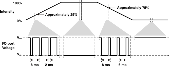
 Figure 25. Output Port Voltage vs LED Intensity, Maximum Intensity = 100%
9.3 System Example
Figure 26 highlights another application where the TPS61052 boost converter and high-power LED driver and TCA6507 7-bit LED driver can be used in combination for applications requiring flashlight functionality, high-brightness indicator and backlight LEDs, or both.
 Figure 26. White LED Flashlight Driver and High-Brightness LED Indicator/Backlight Power Supply