SCPS164D MAY 2007 – February 2017 TCA6507
PRODUCTION DATA.
- 1 Features
- 2 Applications
- 3 Description
- 4 Revision History
- 5 Pin Configuration and Functions
- 6 Specifications
- 7 Parameter Measurement Information
-
8 Detailed Description
- 8.1 Overview
- 8.2 Functional Block Diagram
- 8.3 Feature Description
- 8.4 Device Functional Modes
- 8.5 Programming
- 8.6
Register Maps
- 8.6.1 Registers 0x00 - 0x02 (Select Registers)
- 8.6.2 Register 0x03 (Fade-ON Time)
- 8.6.3 Register 0x04 (Fully-ON Time)
- 8.6.4 Register 0x05 (Fade-OFF Time)
- 8.6.5 Register 0x06 - 0x07 (Fully-OFF Time)
- 8.6.6 Register 0x08 (Maximum Intensity per Bank)
- 8.6.7 Register 0x09 (One-Shot / Master Intensity)
- 8.6.8 Register 0x0A (Initialization Register)
- 9 Application and Implementation
- 10Power Supply Recommendations
- 11Layout
- 12Device and Documentation Support
- 13Mechanical, Packaging, and Orderable Information
Package Options
Mechanical Data (Package|Pins)
Thermal pad, mechanical data (Package|Pins)
- RUE|12
Orderable Information
8 Detailed Description
8.1 Overview
The TCA6507 can be used for driving LEDs and for general-purpose parallel output expansion. The TCA6507 has three select registers (Select0, Select1, and Select2), which can be used to configure each LED output into one of seven different operating modes. At power on, the outputs are in high impedance.
When used to drive LEDs, the seven outputs can be configured into two banks of outputs (BANK0 and BANK1). Each bank of outputs can be independently controlled for dimming rate and intensity through the I2C bus. The dimming and blink rates are fully programmable. The intensity of each bank of LEDs is controlled by dynamically varying the duty cycle of the signal, which has a period of approximately 8 ms and a pulse rate of 125 times per second, driving the outputs. The TCA6507 has two independent dimming-blinking modules—PWM0 and PWM1—driven by a single internal oscillator that supports these features. PWM0 determines the characteristics of BANK0, and PWM1 determines the characteristics of BANK1.
The TCA6507 has a master intensity level known as the ambient light detection (ALD) value. The associated pulse width modulation (PWM) signal for this value is PWMALD. The TCA6507 can be programmed such that PWMALD overrides PWM0 or PWM1, so selected LEDs are on steadily at the master intensity level. Further, the TCA6507 can be programmed such that the ALD value can override the maximum intensity values for PWM0 and PWM1. Thus, the ALD value can control the brightness of all LEDs, whether they are on steadily, or controlled by one of the dimming modules. The ALD value is stored in the lower four bits of the
One-Shot / Master Intensity register.
When the I2C bus is idle, and intensity control is not used, the TCA6507 can be put into shutdown mode by setting the enable (EN) pin low. This mode provides additional power savings, as it is a low-power mode where the LEDs are off. A low signal on the EN pin also resets the registers and I2C/SMBus state machine in the TCA6507 to their default state.
An initial setup command must be sent from the I2C master to the TCA6507 to program the dimming rate and intensity (and intensity ramp if needed) for each bank of outputs. From then on, only one command from the bus master is required to turn each individual output ON, OFF, or to cycle at the programmed dimming rate. The default value for all time parameters is 256 ms, so the default blink rate is approximately one per second.
The TCA6507 is optimized for 1.65 V to 3.6 V on the SDA/SCL side, but the LEDs can be driven by any voltage up to 5.5 V. This allows the TCA6507 to interface with next-generation microprocessors and microcontrollers, where supply levels are dropping down to conserve power.
This LED dimmer supports hot insertion.
8.2 Functional Block Diagram
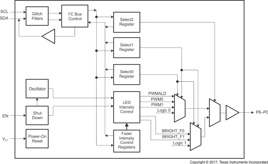 Figure 10. TCA6507 Functional Block Diagram
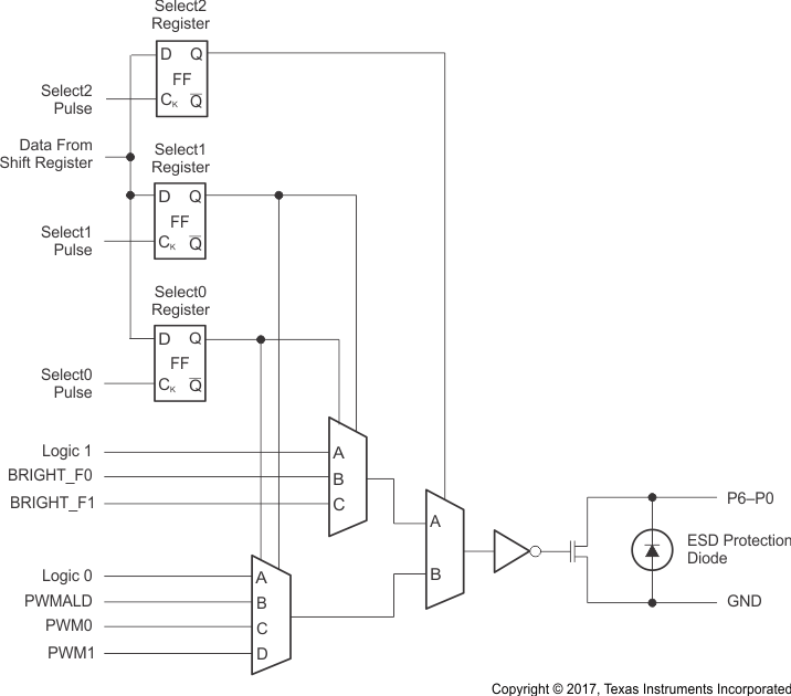 Figure 11. Output Port Simplified Schematic
8.3 Feature Description
8.3.1 Seven LED Driver Outputs
The TCA6507 features 7 outputs that can be controlled with multiple modes: ON, OFF, blinking (one of the two separate banks), and fading at a programmable rate (one of the two separate banks).
8.3.2 Open-Drain Outputs Directly Drive LEDs
The TCA6507 has open-drain outputs (see Figure 11) that are capable of sinking current up to 40 mA for LEDs.
8.3.3 Widely Programmable
The TCA6507 has two separate banks, which can be programmed to do a wide variety of blink rates, fade-ON and fade-OFF rates, as well as maximum intensity (brightness).
8.4 Device Functional Modes
8.4.1 Power-On Reset
When power (from 0 V) is applied to VCC, an internal power-on reset holds the TCA6507 in a reset condition until VCC has reached VPOR. At that point, the reset condition is released, and the TCA6507 registers and I2C/SMBus state machine initialize to their default states.
After the initial power-up phase, VCC must be lowered to below 0.2 V, and then back up to the operating voltage (VCC) for a power-reset cycle.
8.4.2 Enable and Reset
If the enable (EN) input is set to low, the TCA6507 is put in the standby or shutdown mode. In this mode, the oscillator is turned off, the registers are returned to their default state, and the I2C/SMBus state machine is initialized. This mode is useful for low-power consumption. An internal filtering circuit prevents negative glitches from accidentally shutting down the device. EN must be low for a minimum of approximately 60 μs to ensure a shutdown state.
The system master can reset the TCA6507 in the event of a timeout or other improper operation by setting
EN low for a minimum of approximately 60 μs. This has the same effect as a power-on reset without powering-down the TCA6507.
The oscillator start up time (tOSC) is measured from the point when EN is set high.
8.5 Programming
8.5.1 I2C Interface
The TCA6507 has a standard bidirectional I2C interface that is controlled by a master device to be configured or read the status of this device. Each slave on the I2C bus has a specific device address to differentiate between other slave devices that are on the same I2C bus. Many slave devices require configuration upon startup to set the behavior of the device. This is typically done when the master accesses internal register maps of the slave, which have unique register addresses. A device can have one, or multiple registers where data is stored, written, or read.
The physical I2C interface consists of the serial clock (SCL) and serial data (SDA) lines. Both SDA and SCL lines must be connected to VCC through a pullup resistor. The size of the pullup resistor is determined by the amount of capacitance on the I2C lines. For further details, see the I2C Pullup Resistor Calculation application report. Data transfer may be initiated only when the bus is idle. A bus is considered idle if both SDA and SCL lines are high after a STOP condition.
Figure 12 and Figure 13 show the general procedure for a master to access a slave device:
- If a master wants to send data to a slave:
- Master-transmitter sends a START condition and addresses the slave-receiver
- Master-transmitter sends data to slave-receiver
- Master-transmitter terminates the transfer with a STOP condition
- If a master wants to receive or read data from a slave:
- Master-receiver sends a START condition and addresses the slave-transmitter
- Master-receiver sends the requested register to read to slave-transmitter
- Master-receiver receives data from the slave-transmitter
- Master-receiver terminates the transfer with a STOP condition
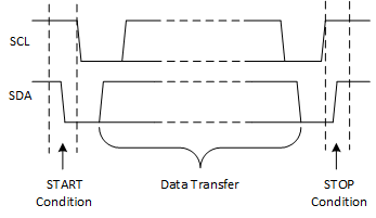 Figure 12. Definition of START and STOP Conditions
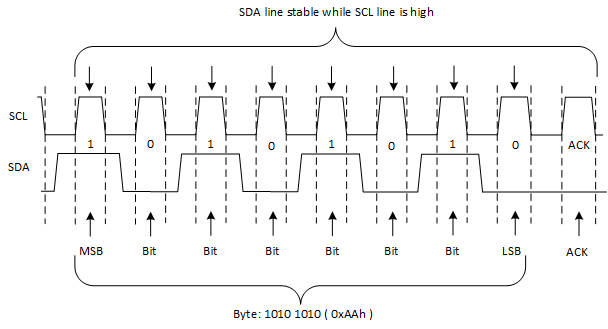 Figure 13. Bit Transfer
8.5.2 Bus Transactions
Data must be sent to and received from the slave devices, and this is accomplished by reading from or writing to registers in the slave device.
Registers are locations in the memory of the slave that contain information, whether it be the configuration information, or some sampled data to send back to the master. The master must write information to these registers to instruct the slave device to perform a task.
8.5.2.1 Writes
To write on the I2C bus, the master sends a START condition on the bus with the address of the slave, as well as the last bit (the R/W bit) set to 0, which signifies a write. After the slave sends the acknowledge bit, the master then sends the register address of the register to which it wishes to write. The slave acknowledges again, letting the master know it is ready. After this, the master starts sending the register data to the slave until the master has sent all the data necessary (which can be only a single byte), and the master terminates the transmission with a STOP condition.
Figure 14 shows an example of writing a single byte to a register.
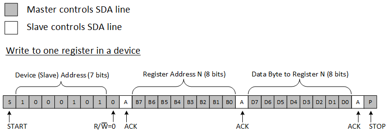 Figure 14. Write to Register
Figure 15 shows an example of writing to a Fully On register.
 Figure 15. Write to the Fully On Register (0x04)
8.5.2.2 Reads
Reading from a slave is very similar to writing, but requires some additional steps. To read from a slave, the master must first instruct the slave which register it wishes to read from. This is done by the master starting off the transmission in a similar fashion as the write, by sending the address with the R/W bit equal to 0 (signifying a write), followed by the register address it wishes to read from. Once the slave acknowledges this register address, the master sends a START condition again, followed by the slave address with the R/W bit set to 1 (signifying a read). This time, the slave acknowledges the read request, and the master releases the SDA bus, but continues supplying the clock to the slave. During this part of the transaction, the master becomes the master-receiver, and the slave becomes the slave-transmitter.
The master continues to send out the clock pulses, but releases the SDA line so that the slave can transmit data. At the end of every byte of data, the master sends an ACK to the slave, letting the slave know that it is ready for more data. Once the master has received the number of bytes it is expecting, it sends a NACK, signaling to the slave to halt communications and release the bus. The master follows this up with a STOP condition.
Figure 16 shows an example of reading a single byte from a slave register.
 Figure 16. Read From Register Example
8.5.3 Device Address
The address of the TCA6507 is shown in Figure 17.
 Figure 17. TCA6507 Address
The last bit of the slave address defines the operation (read or write) to be performed. High (1) selects a read operation, and low (0) selects a write operation. Table 2 shows the TCA6507 interface definition.
Table 2. Interface Definition
| BYTE | BIT | |||||||
|---|---|---|---|---|---|---|---|---|
| 7 (MSB) | 6 | 5 | 4 | 3 | 2 | 1 | 0 (LSB) | |
| I2C slave address | 1 | 0 | 0 | 0 | 1 | 0 | 1 | R/W |
| Px I/O data bus | X(1) | P6 | P5 | P4 | P3 | P2 | P1 | P0 |
8.5.4 Control Register and Command Byte
Following the successful acknowledgment of the address byte, the bus master sends a command byte, which is stored in the control register. The last four bits (B0, B1, B2 and B3) of this command byte determine the internal registers (Select0, Select1, Select2, Fade-ON Time, Fully-ON Time, Fade-OFF Time, First Fully-OFF Time, Second Fully-OFF Time, Maximum Intensity and Initialization) that are affected. The command byte is sent only during a write transmission.
After the command byte is received, the I2C master starts sending data bytes. The first data byte goes into the internal register defined by the command byte. Bit B4 in the command byte is used to determine the programming mode. If B4 is low, all data bytes are written to the register defined by B0, B1, B2, and B3. If B4 is high, the last four bits of the command byte are automatically incremented after the byte is written, and the next data byte is stored in the corresponding register. Registers are written in the sequence shown in Table 6. Once the Initialization register (register 0×0A) is written to, the command byte returns to 0 (Select0 register).
The upper three bits (B7–B5) of the command byte must be programmed as zeroes for proper operation.
If a STOP condition occurs after the command byte is received, the TCA6507 stores the command byte and then remains idle until the I2C master sends the next operation.
Figure 18 shows the TCA6507control register bits.
 Figure 18. Control Register Bits
Table 3 shows the TCA6507 command byte.
Table 3. Command Byte
| BIT | FUNCTION |
|---|---|
| B7 | Reserved. Must be programmed as 0 |
| B6 | Reserved. Must be programmed as 0 |
| B5 | Reserved. Must be programmed as 0 |
| B4 | Auto increment. 1 = Auto increment enabled. 0 = Auto increment disabled |
| B3 | Register address 3 |
| B2 | Register address 2 |
| B1 | Register address 1 |
| B0 | Register address 0 |
8.5.5 Auto-Increment Mode
In auto-increment mode, the last four bits of the command byte are automatically incremented after the byte is written, and the next data byte is stored in the corresponding register. See Figure 19.
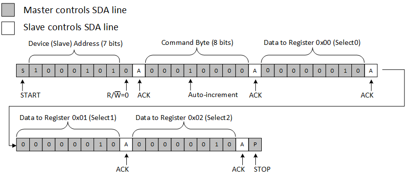 Figure 19.
The registers are written to in the order shown in Table 6.
8.5.6 LED Operation
For LED states, see Figure 10 and Table 8.
It is the combination of Select2, Select1, and Select0 registers that gives the state of the LED or Px.
Bit 0 from the Select0 register, bit = 0 from Select1 register, and bit = 0 from the Select2 register provide the state for P0, or the first LED. Similarly, bit = 1 from the Select0 register, bit 1 from Select1 register, and bit = 1 from the Select2 register provide the state for P1, or the second LED (see Table 4).
Table 4. LED Operation
| MSB | LSB | |||||||
|---|---|---|---|---|---|---|---|---|
| Select0 | X | 0 | 0 | 0 | 0 | 0 | 0 | 0 |
| Select1 | X | 0 | 0 | 0 | 0 | 0 | 0 | 0 |
| Select2 | X | 0 | 0 | 0 | 0 | 0 | 0 | 0 |
| Output or LED affected |
X X |
P6 7th LED |
P5 6th LED |
P4 5th LED |
P3 4th LED |
P2 3rd LED |
P1 2nd LED |
P0 1st LED |
8.5.7 Blinking Pattern Control
The Fade-ON time, Fully-ON time, Fade-OFF time, First Fully-OFF time, and Second Fully-OFF time registers must be written to for basic blink control. Each of these registers has eight bits – top four bits for BANK1 (or PWM1), and bottom four bits for BANK0 (or PWM0) (see Table 20).
Each BANK or PWM has a default value of 4 (4b0100), which translates to a time of 256 ms. The largest value for each BANK or PWM is 15 (4b1111), which translates to a time of 16320 ms (see Figure 20 and Table 5).
Table 5. Intensity Parameters (see Figure 20)
| REGION | PARAMETER NAME | PARAMETER RANGE | REGISTER RANGE | REGISTER NAME | REGISTER |
|---|---|---|---|---|---|
| A1, A2 | Fade-ON time | 0 to 16320 ms (exponential trend) |
0 to 15 | Fade-ON time | 0×03 |
| B1, B2 | Fully-ON time | 0 to 16320 ms (exponential trend) |
0 to 15 | Fully-ON time | 0×04 |
| C1, C2 | Fade-OFF time | 0 to 16320 ms (exponential trend) |
0 to 15 | Fade-OFF time | 0×05 |
| D | First fully-OFF time | 0 to 16320 ms (exponential trend) |
0 to 15 | First fully-OFF time | 0×06 |
| E | Second fully-OFF time | 0 to 16320 ms (exponential trend) |
0 to 15 | Second fully-OFF time | 0×07 |
| F | Maximum intensity | 0 to 100% | 0 to 15 | Maximum intensity | 0×08 |
 Figure 20. LED Pattern Sections Per Bank
Figure 21 and Figure 22 show the output port intensity vs LED intensity.
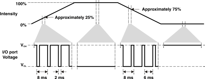 Figure 21. Output Port Voltage vs LED Intensity, Maximum Intensity = 100%
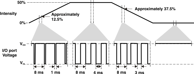 Figure 22. Output Port Voltage vs LED Intensity, Maximum Intensity = 50%
8.5.8 Intensity Control
The Maximum Intensity registers must be written to for setting the intensity of the LED. This register has eight bits – top four bits for BANK1 (or PWM1), and bottom four bits for BANK0 (or PWM0). This register can be written to after sending data to the Second Fully-OFF Time register (see Table 20).
The Maximum Intensity register has a default value of 15 (1111), which translates to 100% brightness
(see Figure 20 and Table 5).
8.6 Register Maps
Table 6 describes the TCA6507 control registers.
Table 6. Control Register Description
| CONTROL REGISTER BITS | COMMAND BYTE (HEX) | REGISTER | PROTOCOL | POWER-UP DEFAULT (BINARY) | |||
|---|---|---|---|---|---|---|---|
| B3 | B2 | B1 | B0 | ||||
| 0 | 0 | 0 | 0 | 0x00 | Select0 | Read/write byte | 0000 0000 |
| 0 | 0 | 0 | 1 | 0x01 | Select1 | Read/write byte | 0000 0000 |
| 0 | 0 | 1 | 0 | 0x02 | Select2 | Read/write byte | 0000 0000 |
| 0 | 0 | 1 | 1 | 0x03 | Fade-ON Time | Read/write byte | 0100 0100 |
| 0 | 1 | 0 | 0 | 0x04 | Fully-ON Time | Read/write byte | 0100 0100 |
| 0 | 1 | 0 | 1 | 0x05 | Fade-OFF Time | Read/write byte | 0100 0100 |
| 0 | 1 | 1 | 0 | 0x06 | First Fully-OFF Time | Read/write byte | 0100 0100 |
| 0 | 1 | 1 | 1 | 0x07 | Second Fully-OFF Time | Read/write byte | 0100 0100 |
| 1 | 0 | 0 | 0 | 0x08 | Maximum Intensity | Read/write byte | 1111 1111 |
| 1 | 0 | 0 | 1 | 0x09 | One Shot / Master Intensity | Read/write byte | 0000 1111 |
| 1 | 0 | 1 | 0 | 0x0A | Initialization | Write byte | N/A |
The Select0 register (register 0x00), Select1 (register 0x01), and Select2 register (register 0x02) configure the state of each of the outputs (see Table 8).
Registers that define time periods have a range of 0 to 16320 ms, as defined in Table 7.
Table 7. Time Parameters
| CODE (DECIMAL) | TIME (ms) |
|---|---|
| 0 | 0 |
| 1 | 64 |
| 2 | 128 |
| 3 | 192 |
| 4 (default) | 256 |
| 5 | 384 |
| 6 | 512 |
| 7 | 768 |
| 8 | 1024 |
| 9 | 1536 |
| 10 | 2048 |
| 11 | 3072 |
| 12 | 4096 |
| 13 | 5760 |
| 14 | 8128 |
| 15 | 16320 |
8.6.1 Registers 0x00 - 0x02 (Select Registers)
Table 8 show the Select2, Select1, and Select0 Register States.
Table 8. Select2, Select1, and Select0 Register States
| SELECT2 | SELECT1 | SELECT0 | STATE |
|---|---|---|---|
| 0 | 0 | 0 | LED off (high impedance). |
| 0 | 0 | 1 | LED off (high impedance). |
| 0 | 1 | 0 | LED on with maximum intensity value of PWM0 (ALD value or BRIGHT_F0 value, depending on One Shot / Master Intensity Register setting). |
| 0 | 1 | 1 | LED on with maximum intensity value of PWM1 (ALD value or BRIGHT_F1 value, depending on One Shot / Master Intensity Register setting). |
| 1 | 0 | 0 | LED fully on (output low). Can be used as general-purpose output. |
| 1 | 0 | 1 | LED on at brightness set by One Shot / Master Intensity register. |
| 1 | 1 | 0 | LED blinking with intensity characteristics of BANK0 (PWM0). |
| 1 | 1 | 1 | LED blinking with intensity characteristics of BANK1 (PWM1). |
Table 9 show the Register 0x00 (Select0 Register).
Table 9. Register 0x00 (Select0 Register)
| BIT | S0-7 | S0-6 | S0-5 | S0-4 | S0-3 | S0-2 | S0-1 | S0-0 |
| DEFAULT | X(1) | 0 | 0 | 0 | 0 | 0 | 0 | 0 |
Table 10 show the Register 0x01 (Select1 Register).
Table 10. Register 0x01 (Select1 Register)
| BIT | S1-7 | S1-6 | S1-5 | S1-4 | S1-3 | S1-2 | S1-1 | S1-0 |
| DEFAULT | X(1) | 0 | 0 | 0 | 0 | 0 | 0 | 0 |
Table 11 show the Register 0x02 (Select2 Register).
Table 11. Register 0x02 (Select2 Register)
| BIT | S2-7 | S2-6 | S2-5 | S2-4 | S2-3 | S2-2 | S2-1 | S2-0 |
| DEFAULT | X(1) | 0 | 0 | 0 | 0 | 0 | 0 | 0 |
To use a P port as a general-purpose output, Select1 and Select0 registers must be set low (or 0), and then the inverse of the data written to the Select2 bit appears on the open-drain output.
The intensity of each bank of LEDs can be customized by programming six registers: Fade-ON Time, Fully-ON Time, Fade-OFF Time, First Fully-OFF Time, Second Fully-OFF Time, and Maximum Intensity registers. Each bank is designed to produce two identical intensity pulses per blink cycle. Both pulses have the same fade-ON, fully-ON and fade-OFF times, but independent fully-OFF times to achieve a double-blink effect when desired.
8.6.2 Register 0x03 (Fade-ON Time)
Table 12 shows the Fade-ON Time Register (Register 0x03).
Table 12. Register 0x03 (Fade-ON Time Register)
| BANK | BANK1 | BANK0 | ||||||
| BIT | C7 | C6 | C5 | C4 | C3 | C2 | C1 | C0 |
| DEFAULT | 0 | 1 | 0 | 0 | 0 | 1 | 0 | 0 |
The Fade-ON Time register (register 0x03) defines the time from the fully-OFF state to the fully-ON state for the LED per region A in Figure 20. The first four bits (C7–C4) in this register set the fade-ON time for BANK1, and the next four bits (C3–C0) set the fade-ON time for BANK0. The data for each bank is a binary number between 0 and 15. For BANK1, the MSB is bit C7, while the least significant bit (LSB) is bit C4. For BANK0, the MSB is bit C3 while the LSB is bit C0. See Table 7 for more information.
8.6.3 Register 0x04 (Fully-ON Time)
Table 13 shows the Fully-ON Time Register (Register 0x04).
Table 13. Register 0x04 (Fully-ON Time Register)
| BANK | BANK1 | BANK0 | ||||||
| BIT | C7 | C6 | C5 | C4 | C3 | C2 | C1 | C0 |
| DEFAULT | 0 | 1 | 0 | 0 | 0 | 1 | 0 | 0 |
The Fully-ON Time register (register 4) defines the time spent at maximum intensity between the fade-ON state and fade-OFF state for the LED per region B in Figure 20. The first four bits (C7–C4) in this register set the
fully-ON time for BANK1, and the next four bits (C3–C0) set the fully-ON time for BANK0. The data for each bank is a binary number between 0 and 15. For BANK1, the MSB is bit C7, while the LSB is bit C4. For BANK0, the most significant bit (MSB) is bit C3, while the LSB is bit C0.
See Table 7 for more information on the possible time values.
8.6.4 Register 0x05 (Fade-OFF Time)
Table 14 shows the Fade-OFF Time Register (Register 0x05).
Table 14. Register 0x05 (Fade-OFF Time Register)
| BANK | BANK1 | BANK0 | ||||||
| BIT | C7 | C6 | C5 | C4 | C3 | C2 | C1 | C0 |
| DEFAULT | 0 | 1 | 0 | 0 | 0 | 1 | 0 | 0 |
The Fade-OFF Time register (register 5) defines the time from the fully-ON state to the fully-OFF state for the LED per region C in Figure 20. The first four bits (C7–C4) in this register set the fade-OFF time for BANK1, and the next four bits (C3–C0) set the fade-OFF time for BANK0. The data for each bank is a binary number between 0 and 15. For BANK1, the MSB is bit C7, while the LSB is bit C4. For BANK0, the MSB is bit C3, while the least significant bit (LSB) is bit C0.
See Table 7 for more information on the possible time values.
8.6.5 Register 0x06 - 0x07 (Fully-OFF Time)
Table 15 and Table 16 show the Fully-OFF Time register (Register 0x06 - 0x07).
Table 15. Register 0x06 (First Fully-OFF Time Register)
| BANK | BANK1 | BANK0 | ||||||
| BIT | C7 | C6 | C5 | C4 | C3 | C2 | C1 | C0 |
| DEFAULT | 0 | 1 | 0 | 0 | 0 | 1 | 0 | 0 |
Table 16. Register 0x07 (Second Fully-OFF Time Register)
| BANK | BANK1 | BANK0 | ||||||
| BIT | C7 | C6 | C5 | C4 | C3 | C2 | C1 | C0 |
| DEFAULT | 0 | 1 | 0 | 0 | 0 | 1 | 0 | 0 |
The first and second Fully-OFF Time registers (registers 6 and 7) define the time spent at zero intensity (in the fully-OFF state of the LED) per region D and E, respectively, in Figure 20. The first four bits (C7–C4) in this register set the fully-OFF time for BANK1, and the next four bits (C3–C0) set the fully-OFF time for BANK0. The data for each bank is a binary number between 0 and 15. For BANK1, the MSB is bit C7, while the LSB is bit C4. For BANK0, the MSB is bit C3, while the LSB is bit C0.
See Table 7 for more information on the possible time values.
8.6.6 Register 0x08 (Maximum Intensity per Bank)
Table 17 shows the Maximum Intensity Register (Register 0x08).
Table 17. Register 0x08 (Maximum Intensity Register)
| BANK | BANK1 | BANK0 | ||||||
| BIT | C7 | C6 | C5 | C4 | C3 | C2 | C1 | C0 |
| DEFAULT | 1 | 1 | 1 | 1 | 1 | 1 | 1 | 1 |
The Maximum Intensity register defines the duty cycle of the waveform driving the LED in its fully-ON state per region F in Figure 20. The first four bits (C7–C4) in this register set the duty cycle for BANK1 and the next four bits (C3–C0) set the duty cycle for BANK0. The data for each bank is a binary number between 0 and 15. For BANK1, the MSB is bit C7, while the LSB is bit C4. For BANK0, the MSB is bit C3, while the LSB is bit C0. The values in this register also define the LED intensity indicated by the BRIGHT_F0 or BRIGHT_F1 modes. The intensity of each LED is updated 125 times per second (every 8 ms with a 32-kHz clock).
The values for each value are shown in Table 18.
Table 18. Brightness Register Values
| Code | Brightness | |
|---|---|---|
| Decimal | Nibble (Hex) | |
| 0 | 0x0 | 0 % |
| 1 | 0x1 | 6.67% |
| 2 | 0x2 | 13.33% |
| 3 | 0x3 | 20.00% |
| 4 | 0x4 | 26.67 % |
| 5 | 0x5 | 33.33 % |
| 6 | 0x6 | 40.00 % |
| 7 | 0x7 | 46.67 % |
| 8 | 0x8 | 53.33 % |
| 9 | 0x9 | 60.00 % |
| 10 | 0xA | 66.67 % |
| 11 | 0xB | 73.33 % |
| 12 | 0xC | 80.00 % |
| 13 | 0xD | 86.67 % |
| 14 | 0xE | 93.33 % |
| 15 | 0xF | 100 % |
8.6.7 Register 0x09 (One-Shot / Master Intensity)
The One-Shot / Master Intensity register (register 9) is an 8-bit register with three functions.
Bits 0–3 set the master intensity value (ALD). It is a binary number between 0 and 15.
Bits 4–5 determine whether the maximum intensity of PWM0 and PWM1 is set by the programmed F value (BRIGHT_F0 or BRIGHT_F1) or the master ALD value. The default value for these bits is 0. Bit 4 supports PWM0 and bit 5 is for PWM1. If bit 4 (or bit 5) is 0, the maximum intensity value for PWM0 (or PWM1) is set by the F value. If bit 4 (or bit 5) is 1, the maximum intensity value for PWM0 (or PWM1) is set by the master ALD value. This allows the user to vary the brightness of all LEDs by changing a single register.
Bits 6–7 determine whether each PWM operates in normal or one-shot mode. Bit 6 supports PWM0 and bit 7 is for PWM1. If bit 6 (or bit 7) is 0, PWM0 (or PWM1) operates in the normal mode where the LEDs goes through the full intensity cycle defined by Table 5 and Figure 20. If bit 6 (or bit 7) is 1, PWM0 (or PWM1) operate in the one-shot mode. In this mode, the LEDs can be used to create a single-shot lighting effect where the LED intensity is valid for a particular segment of the cycle shown in Table 5 and Figure 20. As a note for users who plan to use one-shot mode, the time register corresponding to the sections for the desired one-shot starting location, and immediately after must both have non-zero values in the registers for time in order for one-shot to function as expected.
Table 19 shows the One-Shot / Master Intensity Register.
Table 19. One-Shot / Master Intensity Register
| BIT | DESCRIPTION |
|---|---|
| 0–3 | Master intensity (ALD) value. Valid values are 0 to 15. See Table 18 for more information |
| 4 | Determines whether maximum intensity of PWM0 is set by the programmed F value or the master ALD value 0 = F value 1 = ALD value |
| 5 | Determines whether maximum intensity of PWM1 is set by the programmed F value or the master ALD value 0 = F value defined in Maximum Intensity per Bank Register (0x08) 1 = ALD value |
| 6 | Determines if PWM0 operates in normal or one-shot mode 0 = Normal mode 1 = One-shot mode |
| 7 | Determines if PWM1 operates in normal or one-shot mode 0 = Normal mode 1 = One-shot mode |
8.6.8 Register 0x0A (Initialization Register)
The Initialization register (register 0x0A) determines whether to initialize each PWM and, if so, provides the starting point of the LED intensity cycle for each bank. Bits 0–3 (C0–C3) are for BANK0 and bits 4–7 (C4–C7) are for BANK1. Table 20 shws the Initialization Register (Register 0x0A).
Bits 0–2 provide the starting point for PWM0. If bit 3 is high (or 1), it initializes PWM0.
Bits 4–6 provide the starting point for PWM1. If bit 7 is high (or 1), it initialized PWM1.
In the one-shot mode for BANK0, the LEDs start at the beginning of the region defined by C2, C1, and C0 in the Initialization register and, when it reaches the end of that region, the LED stays at that intensity level defined at the end of the region. When the stop point is reached, all P ports attached to PWM0 disconnect from PWM0, and stay at either the maximum intensity level for PWM0 (BRIGHT_F0 or ALD value), or the OFF state. The bits in the Select2 and Select1 registers change to reflect the final state of the LED at that time. PWM0 continues running, and is free to be used by other LEDs. The one-shot mode works similarly for BANK1.
Upon writing to this register, each bank is initialized to the state listed in Table 21 and Table 22.
Table 20. Register 0x0A (Initialization Register)
| BANK | BANK1 | BANK0 | ||||||
| BIT | C7 | C6 | C5 | C4 | C3 | C2 | C1 | C0 |
Table 21. Bank 1 Initialization Register
| C7 | C6 | C5 | C4 | INTENSITY CYCLE |
|---|---|---|---|---|
| 1 | 0 | 0 | 0 | Beginning at region A1 in Table 5 and Figure 18 |
| 1 | 0 | 0 | 1 | Beginning at region B1 in Table 5 and Figure 18 |
| 1 | 0 | 1 | 0 | Beginning at region C1 in Table 5 and Figure 18 |
| 1 | 0 | 1 | 1 | Beginning at region D in Table 5 and Figure 18 |
| 1 | 1 | 0 | 0 | Beginning at region A2 in Table 5 and Figure 18 |
| 1 | 1 | 0 | 1 | Beginning at region B2 in Table 5 and Figure 18 |
| 1 | 1 | 1 | 0 | Beginning at region C2 in Table 5 and Figure 18 |
| 1 | 1 | 1 | 1 | Beginning at region E in Table 5 and Figure 18 |
Table 22. Bank 0 Initialization Register
| C3 | C2 | C1 | C0 | STARTING POINT OF INTENSITY CYCLE |
|---|---|---|---|---|
| 1 | 0 | 0 | 0 | Beginning at region A1 in Table 5 and Figure 18 |
| 1 | 0 | 0 | 1 | Beginning at region B1 in Table 5 and Figure 18 |
| 1 | 0 | 1 | 0 | Beginning at region C1 in Table 5 and Figure 18 |
| 1 | 0 | 1 | 1 | Beginning at region D in Table 5 and Figure 18 |
| 1 | 1 | 0 | 0 | Beginning at region A2 in Table 5 and Figure 18 |
| 1 | 1 | 0 | 1 | Beginning at region B2 in Table 5 and Figure 18 |
| 1 | 1 | 1 | 0 | Beginning at region C2 in Table 5 and Figure 18 |
| 1 | 1 | 1 | 1 | Beginning at region E in Table 5 and Figure 18 |