SCPS233E March 2012 – February 2017 TCA9554
PRODUCTION DATA.
- 1 Features
- 2 Applications
- 3 Description
- 4 Revision History
- 5 Pin Configuration and Functions
- 6 Specifications
- 7 Parameter Measurement Information
- 8 Detailed Description
- 9 Application and Implementation
- 10Power Supply Recommendations
- 11Layout
- 12Device and Documentation Support
- 13Mechanical, Packaging, and Orderable Information
Package Options
Mechanical Data (Package|Pins)
Thermal pad, mechanical data (Package|Pins)
- DW|16
Orderable Information
9 Application and Implementation
NOTE
Information in the following applications sections is not part of the TI component specification, and TI does not warrant its accuracy or completeness. TI’s customers are responsible for determining suitability of components for their purposes. Customers should validate and test their design implementation to confirm system functionality.
9.1 Application Information
Applications of the TCA9554 has this device connected as a slave to an I2C master (processor), and the I2C bus may contain any number of other slave devices. The TCA9554 is typically in a remote location from the master, placed close to the GPIOs to which the master must monitor or control.
IO Expanders such as the TCA9554 are typically used for controlling LEDs (for feedback or status lights), controlling enable or reset signals of other devices, and even reading the outputs of other devices or buttons.
9.2 Typical Application
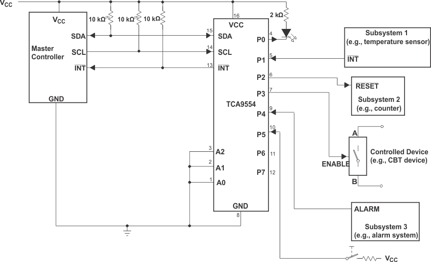
Figure 26 shows an application in which the TCA9554 can be used.
9.2.1 Design Requirements
9.2.1.1 Calculating Junction Temperature and Power Dissipation
When designing with this device, it is important that the Recommended Operating Conditions not be violated. Many of the parameters of this device are rated based on junction temperature. So junction temperature must be calculated in order to verify that safe operation of the device is met. The basic equation for junction temperature is shown in Equation 1.

θJA is the standard junction to ambient thermal resistance measurement of the package, as seen in Thermal Information table. Pd is the total power dissipation of the device, and the approximation is shown in Equation 2.

Equation 2 is the approximation of power dissipation in the device. The equation is the static power plus the summation of power dissipated by each port (with a different equation based on if the port is outputting high, or outputting low. If the port is set as an input, then power dissipation is the input leakage of the pin multiplied by the voltage on the pin). Note that this ignores power dissipation in the INT and SDA pins, assuming these transients to be small. They can easily be included in the power dissipation calculation by using Equation 3 to calculate the power dissipation in INT or SDA while they are pulling low, and this gives maximum power dissipation.

Equation 3 shows the power dissipation for a single port which is set to output low. The power dissipated by the port is the VOL of the port multiplied by the current it is sinking.

Equation 4 shows the power dissipation for a single port which is set to output high. The power dissipated by the port is the current sourced by the port multiplied by the voltage drop across the device (difference between VCC and the output voltage).
9.2.1.2 Minimizing ICC when I/Os Control LEDs
When the I/Os are used to control LEDs, normally they are connected to VCC through a resistor as shown in Figure 26. For a P-port configured as an input, ICC increases as VI becomes lower than VCC. The LED is a diode, with threshold voltage VT, and when a P-port is configured as an input the LED is off but VI is a VT drop below VCC.
For battery-powered applications, it is essential that the voltage of P-ports controlling LEDs is greater than or equal to VCC when the P-ports are configured as input to minimize current consumption. Figure 27 shows a high-value resistor in parallel with the LED. Figure 28 shows VCC less than the LED supply voltage by at least VT. Both of these methods maintain the I/O VI at or above VCC and prevents additional supply current consumption when the P-port is configured as an input and the LED is off.
The TCA9554 has an integrated 100-kΩ pull-up resistor, so there is no need for an external pull-up.
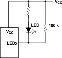 Figure 27. High-Value Resistor in Parallel With LED
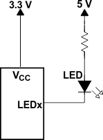 Figure 28. Device Supplied by a Lower Voltage
9.2.2 Detailed Design Procedure
The pull-up resistors, RP, for the SCL and SDA lines need to be selected appropriately and take into consideration the total capacitance of all slaves on the I2C bus. The minimum pull-up resistance is a function of VCC, VOL,(max), and IOL as shown in Equation 5.

The maximum pull-up resistance is a function of the maximum rise time, tr (300 ns for fast-mode operation, fSCL = 400 kHz) and bus capacitance, Cb as shown in Equation 6.

The maximum bus capacitance for an I2C bus must not exceed 400 pF for standard-mode or fast-mode operation. The bus capacitance can be approximated by adding the capacitance of the TCA9554, Ci for SCL or Cio for SDA, the capacitance of wires, connections, traces, and the capacitance of additional slaves on the bus.
9.2.3 Application Curves
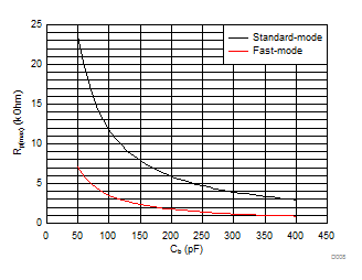
| Standard-mode (fSCL= 100 kHz, tr = 1 µs) |
Fast-mode (fSCL = 400 kHz, tr = 300 ns) |
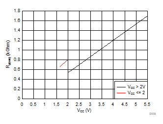
| VOL = 0.2 × VCC, IOL = 2 mA when VCC ≤ 2 V | ||
| VOL = 0.4 V, IOL = 3 mA when VCC > 2 V |