SCPS233E March 2012 – February 2017 TCA9554
PRODUCTION DATA.
- 1 Features
- 2 Applications
- 3 Description
- 4 Revision History
- 5 Pin Configuration and Functions
- 6 Specifications
- 7 Parameter Measurement Information
- 8 Detailed Description
- 9 Application and Implementation
- 10Power Supply Recommendations
- 11Layout
- 12Device and Documentation Support
- 13Mechanical, Packaging, and Orderable Information
Package Options
Mechanical Data (Package|Pins)
Thermal pad, mechanical data (Package|Pins)
- DW|16
Orderable Information
8 Detailed Description
8.1 Overview
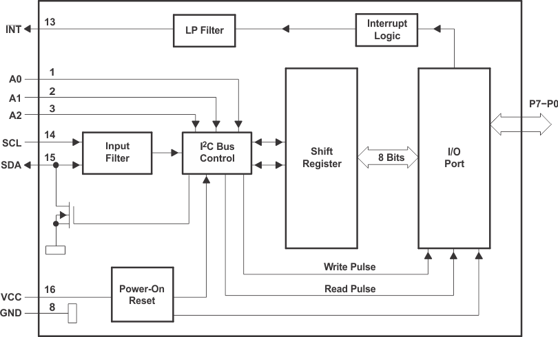
The TCA9554 is an 8-bit I/O expander for the two-line bidirectional bus (I2C) is designed for 1.65-V to 5.5-V VCC operation. It provides general-purpose remote I/O expansion for most micro-controller families via the I2C interface (serial clock, SCL, and serial data, SDA, pins).
The TCA9554 open-drain interrupt (INT) output is activated when any input state differs from its corresponding Input Port register state and is used to indicate to the system master that an input state has changed. The INT pin can be connected to the interrupt input of a micro-controller. By sending an interrupt signal on this line, the remote I/O can inform the micro-controller if there is incoming data on its ports without having to communicate via the I2C bus. Thus, the TCA9554 can remain a simple slave device. The device outputs (latched) have high-current drive capability for directly driving LEDs.
Three hardware pins (A0, A1, and A2) are used to program and vary the fixed I2C slave address and allow up to eight devices to share the same I2C bus or SMBus.
The system master can reset the TCA9554 in the event of a timeout or other improper operation by cycling the power supply and causing a power-on reset (POR). A reset puts the registers in their default state and initializes the I2C /SMBus state machine.
The TCA9554 consists of one 8-bit Configuration (input or output selection), Input Port, Output Port, and Polarity Inversion (active high or active low) registers. At power on, the I/Os are configured as inputs. However, the system master can enable the I/Os as either inputs or outputs by writing to the I/O configuration bits. The data for each input or output is kept in the corresponding Input Port or Output Port register. The polarity of the Input Port register can be inverted with the Polarity Inversion register. All registers can be read by the system master.
The TCA9554 and TCA9554A are identical except for their fixed I2C address. This allows for up to 16 of these devices (8 of each) on the same I2C/SMBus.
The TCA9554 is identical to the TCA9534 except for the addition of the internal I/O pull-up resistors, which keeps P-ports from floating when configured as inputs.
8.2 Functional Block Diagram
8.3 Feature Description
8.3.1 I/O Port
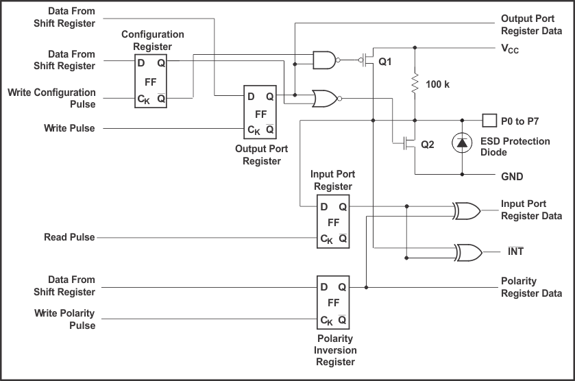
When an I/O is configured as an input, FETs Q1 and Q2 are off, creating a high-impedance input with a weak pull-up (100 kΩ typical) to VCC. The input voltage may be raised above VCC to a maximum of 5.5 V, however it must be noted that because of the integrated 100 kΩ pull-up resistor it may result in current flow from I/O to VCC pin (Figure 15).
If the I/O is configured as an output, Q1 or Q2 is enabled depending on the state of the output port register. In this case, there are low impedance paths between the I/O pin and either VCC or GND. The external voltage applied to this I/O pin must not exceed the recommended levels for proper operation.
8.3.2 Interrupt Output (INT)
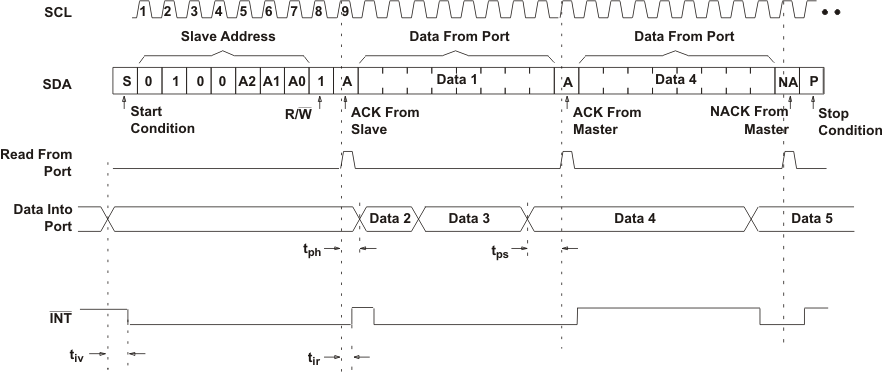
An interrupt is generated by any rising or falling edge of any P-port I/O configured as an input. After time tiv, the signal INT is valid. Resetting the interrupt circuit is achieved when data on the ports is changed back to the original state or when data is read from the Input Port register. Resetting occurs in the read mode at the acknowledge (ACK) bit after the rising edge of the SCL signal. Interrupts that occur during the ACK clock pulse can be lost (or be very short) due to the resetting of the interrupt during this pulse. Each change of the I/Os after resetting is detected and is transmitted as an interrupt on the INT pin.
Reading from or writing to another device does not affect the interrupt circuit, and a pin configured as an output cannot cause an interrupt. Changing an I/O from an output to an input may cause a false interrupt to occur if the state of the pin does not match the contents of the Input Port register.
The INT output has an open-drain structure and requires pull-up resistor to VCC.
8.4 Device Functional Modes
8.4.1 Power-On Reset
When power (from 0 V) is applied to VCC, an internal power-on reset holds the TCA9554 in a reset condition until VCC has reached VPORR. At that point, the reset condition is released and the TCA9554 registers and SMBus/I2C state machine initializes to their default states. After that, VCC must be lowered to below VPORF and then back up to the operating voltage for a power-on reset cycle.
8.5 Programming
8.5.1 I2C Interface
The bidirectional I2C bus consists of the serial clock (SCL) and serial data (SDA) lines. Both lines must be connected to a positive supply through a pull-up resistor when connected to the output stages of a device. Data transfer may be initiated only when the bus is not busy.
I2C communication with this device is initiated by a master sending a Start condition, a high-to-low transition on the SDA input-output while the SCL input is high (see Figure 16). After the Start condition, the device address byte is sent, most significant bit (MSB) first, including the data direction bit (R/W).
After receiving the valid address byte, this device responds with an acknowledge (ACK), a low on the SDA input/output during the high of the ACK-related clock pulse. The address inputs (A0–A2) of the slave device must not be changed between the Start and the Stop conditions.
On the I2C bus, only one data bit is transferred during each clock pulse. The data on the SDA line must remain stable during the high pulse of the clock period, as changes in the data line at this time are interpreted as control commands (Start or Stop) (see Figure 17).
A Stop condition, a low-to-high transition on the SDA input/output while the SCL input is high, is sent by the master (see Figure 16).
Any number of data bytes can be transferred from the transmitter to receiver between the Start and the Stop conditions. Each byte of eight bits is followed by one ACK bit. The transmitter must release the SDA line before the receiver can send an ACK bit. The device that acknowledges must pull down the SDA line during the ACK clock pulse so that the SDA line is stable low during the high pulse of the ACK-related clock period (see Figure 18). When a slave receiver is addressed, it must generate an ACK after each byte is received. Similarly, the master must generate an ACK after each byte that it receives from the slave transmitter. Setup and hold times must be met to ensure proper operation.
A master receiver signals an end of data to the slave transmitter by not generating an acknowledge (NACK) after the last byte has been clocked out of the slave. This is done by the master receiver by holding the SDA line high. In this event, the transmitter must release the data line to enable the master to generate a Stop condition.
 Figure 16. Definition of Start and Stop Conditions
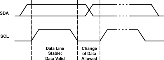 Figure 17. Bit Transfer
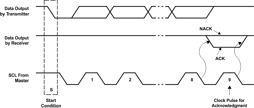 Figure 18. Acknowledgment on I2C Bus
Table 1 shows the TCA9554 interface definition.
Table 1. Interface Definition Table
| BYTE | BIT | |||||||
|---|---|---|---|---|---|---|---|---|
| 7 (MSB) | 6 | 5 | 4 | 3 | 2 | 1 | 0 (LSB) | |
| I2C slave address | L | H | L | L | A2 | A1 | A0 | R/W |
| Px I/O data bus | P7 | P6 | P5 | P4 | P3 | P2 | P1 | P0 |
8.6 Register Maps
8.6.1 Device Address
Figure 19 shows the address byte of the TCA9554.
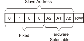 Figure 19. TCA9554 Address
Table 2 shows the TCA9554 address reference.
Table 2. Address Reference
| INPUTS | I2C BUS SLAVE ADDRESS | ||
|---|---|---|---|
| A2 | A1 | A0 | |
| L | L | L | 32 (decimal), 20 (hexadecimal) |
| L | L | H | 33 (decimal), 21 (hexadecimal) |
| L | H | L | 34 (decimal), 22 (hexadecimal) |
| L | H | H | 35 (decimal), 23 (hexadecimal) |
| H | L | L | 36 (decimal), 24 (hexadecimal) |
| H | L | H | 37 (decimal), 25 (hexadecimal) |
| H | H | L | 38 (decimal), 26 (hexadecimal) |
| H | H | H | 39 (decimal), 27 (hexadecimal) |
The last bit of the slave address defines the operation (read or write) to be performed. When it is high (1), a read is selected, while a low (0) selects a write operation.
8.6.2 Control Register and Command Byte
Following the successful Acknowledgment of the address byte, the bus master sends a command byte that is stored in the control register in the TCA9554 (see Figure 20). Two bits of this command byte state the operation (read or write) and the internal register (input, output, polarity inversion or configuration) that is affected. This register can be written or read through the I2C bus. The command byte is sent only during a write transmission.
Once a command byte has been sent, the register that was addressed continues to be accessed by reads until a new command byte has been sent.
 Figure 20. Control Register Bits
Table 3 shows the TCA9554 command byte.
Table 3. Command Byte Table
| CONTROL REGISTER BITS | COMMAND BYTE (HEX) | REGISTER | PROTOCOL | POWER-UP DEFAULT | |
|---|---|---|---|---|---|
| B1 | B0 | ||||
| 0 | 0 | 0×00 | Input Port | Read byte | XXXX XXXX |
| 0 | 1 | 0×01 | Output Port | Read-write byte | 1111 1111 |
| 1 | 0 | 0×02 | Polarity Inversion | Read-write byte | 0000 0000 |
| 1 | 1 | 0×03 | Configuration | Read-write byte | 1111 1111 |
8.6.3 Register Descriptions
The Input Port register (register 0) reflects the incoming logic levels of the pins, regardless of whether the pin is defined as an input or an output by the Configuration register. It only acts on read operation. Writes to these registers have no effect. The default value, X, is determined by the externally applied logic level.
Before a read operation, a write transmission is sent with the command byte to indicate to the I2C device that the Input Port register is accessed next. See Table 4.
Table 4. Register 0 (Input Port Register) Table
| BIT | I7 | I6 | I5 | I4 | I3 | I2 | I1 | I0 |
| DEFAULT | X | X | X | X | X | X | X | X |
The Output Port register (register 1) shows the outgoing logic levels of the pins defined as outputs by the Configuration register. Bit values in this register have no effect on pins defined as inputs. In turn, reads from this register reflect the value that is in the flip-flop controlling the output selection, not the actual pin value. See Table 5.
Table 5. Register 1 (Output Port Register) Table
| BIT | O7 | O6 | O5 | O4 | O3 | O2 | O1 | O0 |
| DEFAULT | 1 | 1 | 1 | 1 | 1 | 1 | 1 | 1 |
The Polarity Inversion register (register 2) allows polarity inversion of pins defined as inputs by the Configuration register. If a bit in this register is set (written with 1), the corresponding port pin polarity is inverted. If a bit in this register is cleared (written with a 0), the corresponding port pin original polarity is retained. See Table 6.
Table 6. Register 2 (Polarity Inversion Register) Table
| BIT | N7 | N6 | N5 | N4 | N3 | N2 | N1 | N0 |
| DEFAULT | 0 | 0 | 0 | 0 | 0 | 0 | 0 | 0 |
The Configuration register (register 3) configures the directions of the I/O pins. If a bit in this register is set to 1, the corresponding port pin is enabled as an input with a high-impedance output driver. If a bit in this register is cleared to 0, the corresponding port pin is enabled as an output. See Table 7.
Table 7. Register 3 (Configuration Register) Table
| BIT | C7 | C6 | C5 | C4 | C3 | C2 | C1 | C0 |
| DEFAULT | 1 | 1 | 1 | 1 | 1 | 1 | 1 | 1 |
8.6.3.1 Bus Transactions
Data is exchanged between the master and the TCA9554 through write and read commands.
8.6.3.1.1 Writes
To write on the I2C bus, the master sends a START condition on the bus with the address of the slave, as well as the last bit (the R/W bit) set to 0, which signifies a write. After the slave sends the acknowledge bit, the master then sends the register address of the register to which it wishes to write. The slave acknowledges again, letting the master know it is ready. After this, the master starts sending the register data to the slave until the master has sent all the data necessary (which is sometimes only a single byte), and the master terminates the transmission with a STOP condition. Note that the command byte/register address does NOT automatically increment. Writing multiple bytes during a write results in the last byte sent being stored in the register.
See the Register Descriptions section to see list of the TCA9554's internal registers and a description of each one.
Figure 21 shows an example of writing a single byte to a slave register.
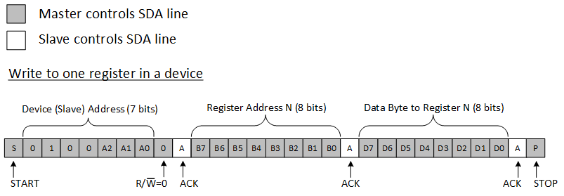 Figure 21. Write to Register
Figure 22 shows an example of how to write to the polarity inversion register.
 Figure 22. Write to the Polarity Inversion Register
Figure 23 shows an example of how to write to output port register.
 Figure 23. Write to Output Port Register
8.6.3.1.2 Reads
The bus master first must send the TCA9554 address with the LSB set to a logic 0 (see Figure 19 for device address). The command byte is sent after the address and determines which register is accessed. After a restart, the device address is sent again but, this time, the LSB is set to a logic 1. Data from the register defined by the command byte then is sent by the TCA9554 (see Figure 25). The command byte does not increment automatically. If multiple bytes are read, data from the specified command byte/register is going to be continuously read.
See the Register Descriptions section for the list of the TCA9554's internal registers and a description of each one.
Figure 24 shows an example of reading a single byte from a slave register.
 Figure 24. Read from Register
After a restart, the value of the register defined by the command byte matches the register being accessed when the restart occurred. Data is clocked into the register on the rising edge of the ACK clock pulse. After the first byte, additional bytes may be read, but the same register specified by the command byte is read.
Data is clocked into the register on the rising edge of the ACK clock pulse. There is no limitation on the number of data bytes received in one read transmission, but when the final byte is received, the bus master must not acknowledge the data.
