SCPS280A November 2022 – November 2023 TCAL9538
PRODUCTION DATA
- 1
- 1 Features
- 2 Applications
- 3 Description
- 4 Pin Configuration and Functions
- 5 Specifications
- 6 Parameter Measurement Information
- 7 Detailed Description
- 8 Application and Implementation
- 9 Device and Documentation Support
- 10Revision History
- 11Mechanical, Packaging, and Orderable Information
Package Options
Refer to the PDF data sheet for device specific package drawings
Mechanical Data (Package|Pins)
- PW|16
- DTU|16
- RSV|16
Thermal pad, mechanical data (Package|Pins)
Orderable Information
4 Pin Configuration and Functions
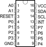
 Figure 4-1 PW (TSSOP) Package,
16-Pin
Figure 4-1 PW (TSSOP) Package,
16-Pin(Top View)
 Figure 4-3 DTU (X2QFN) Package,
16-Pin
Figure 4-3 DTU (X2QFN) Package,
16-Pin(Top View)
 Figure 4-2 RSV (UQFN) Package,
16-Pin
Figure 4-2 RSV (UQFN) Package,
16-Pin(Top View)
Table 4-1 Pin Functions
| PIN | TYPE(1) | DESCRIPTION | |||
|---|---|---|---|---|---|
| NAME | TSSOP (PW) |
QFN (RSV) |
X2QFN (DTU) |
||
| A0 | 1 | 15 | A2 | I | Address input. Connect directly to VCC or ground |
| A1 | 2 | 16 | B2 | I | Address input. Connect directly to VCC or ground |
| GND | 8 | 6 | D2 | – | Ground |
| INT | 13 | 11 | B4 | O | Interrupt output. Connect to VCC through a pull-up resistor |
| P0 | 4 | 2 | B1 | I/O | P-port input/output (push-pull design structure). At power on, P0 is configured as an input |
| P1 | 5 | 3 | C2 | I/O | P-port input/output (push-pull design structure). At power on, P1 is configured as an input |
| P2 | 6 | 4 | C1 | I/O | P-port input/output (push-pull design structure). At power on, P2 is configured as an input |
| P3 | 7 | 5 | D1 | I/O | P-port input/output (push-pull design structure). At power on, P3 is configured as an input |
| P4 | 9 | 7 | D3 | I/O | P-port input/output (push-pull design structure). At power on, P4 is configured as an input |
| P5 | 10 | 8 | D4 | I/O | P-port input/output (push-pull design structure). At power on, P5 is configured as an input |
| P6 | 11 | 9 | C4 | I/O | P-port input/output (push-pull design structure). At power on, P6 is configured as an input |
| P7 | 12 | 10 | C3 | I/O | P-port input/output (push-pull design structure). At power on, P7 is configured as an input |
| RESET | 3 | 1 | A1 | I | Active-low reset input. Connect to VCC through a pull-up resistor, if no active connection is used |
| SCL | 14 | 12 | A4 | I | Serial clock bus. Connect to VCC through a pull-up resistor |
| SDA | 15 | 13 | B3 | I/O | Serial data bus. Connect to VCC through a pull-up resistor |
| VCC | 16 | 14 | A3 | – | Supply voltage |
(1) I = Input, O = Output, I/O =
Input or Output.