SBOS766B February 2016 – February 2016 THS3217
PRODUCTION DATA.
- 1 Features
- 2 Applications
- 3 Description
- 4 Revision History
- 5 Device Comparison Table
- 6 Pin Configuration and Functions
-
7 Specifications
- 7.1 Absolute Maximum Ratings
- 7.2 ESD Ratings
- 7.3 Recommended Operating Conditions
- 7.4 Thermal Information
- 7.5 Electrical Characteristics: D2S
- 7.6 Electrical Characteristics: OPS
- 7.7 Electrical Characteristics: D2S + OPS
- 7.8 Electrical Characteristics: Midscale (DC) Reference Buffer
- 7.9 Typical Characteristics: D2S + OPS
- 7.10 Typical Characteristics: D2S Only
- 7.11 Typical Characteristics: OPS only
- 7.12 Typical Characteristics: Midscale (DC) Reference Buffer
- 7.13 Typical Characteristics: Switching Performance
- 7.14 Typical Characteristics: Miscellaneous Performance
- 8 Parameter Measurement Information
-
9 Detailed Description
- 9.1 Overview
- 9.2 Functional Block Diagram
- 9.3 Feature Description
- 9.4 Device Functional Modes
-
10Application and Implementation
- 10.1
Application Information
- 10.1.1
Typical Applications
- 10.1.1.1 High-Frequency, High-Voltage, Dual-Output Line Driver for AWGs
- 10.1.1.2 High-Voltage Pulse-Generator
- 10.1.1.3 Single-Supply, AC-Coupled, Piezo Element Driver
- 10.1.1.4 Output Common-Mode Control Using the Midscale Buffer as a Level Shifter
- 10.1.1.5 Differential I/O Driver With independent Common-Mode Control
- 10.1.1
Typical Applications
- 10.1
Application Information
- 11Power Supply Recommendations
- 12Layout
- 13Device and Documentation Support
- 14Mechanical, Packaging, and Orderable Information
Package Options
Mechanical Data (Package|Pins)
- RGV|16
Thermal pad, mechanical data (Package|Pins)
- RGV|16
Orderable Information
8 Parameter Measurement Information
8.1 Overview
The THS3217 comprises three blocks of high-performance amplifiers. Each block requires both frequency-response and step-response characterization. The midscale buffer and OPS use standard, single-ended I/O test methods with network analyzers, pulse generators, and high-speed oscilloscopes. The differential to single-ended input stage (D2S) requires a wideband differential source for test purposes. All ac characterization tests were performed using the THS3217 evaluation module (EVM), the THS3217EVM, which offers many configuration options. For most of the D2S-only tests, the OPS was disabled. Figure 67 shows a typical configuration for an ac frequency-response test of the D2S.
The THS3217EVM includes unpopulated, optional, passive elements at the D2S inputs to implement a differential filter. These elements were not used in the D2S characterization and the two input pins were terminated to ground through 49.9-Ω resistors. DC test points are provided through 10-kΩ or 20-kΩ resistors on all THS3217 nodes. Figure 67 also shows the output network used to emulate a 200-Ω load resistance (RLOAD) while presenting a 50-Ω source back to the D2S output pin. The R3 (= 169 Ω) and R4 (= 73.2 Ω) resistors combine with the 50-Ω network analyzer input impedance to present a 200-Ω load at VO1 (pin 6), The impedance presented from the input of the network analyzer back to the D2S output (VO1, pin 6) is 50-Ω. The 16.5-dB insertion loss intrinsic to this dc-coupled impedance network is removed from the characterization curves. The VREF pin was connected to GND for all the tests.
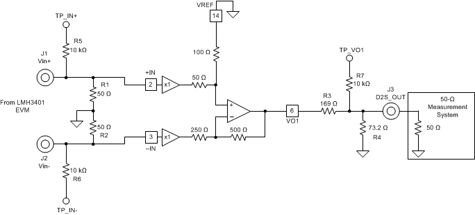 Figure 67. D2S Input and Output Interface Showing 50-Ω Differential Input, 200-Ω RLOAD at VO1
8.2 Frequency Response Measurement
For D2S and full-signal path (D2S + OPS) characterization, the LMH3401, a very wideband, dc-coupled, single-ended to differential amplifier was used. The LMH3401EVM was used as an interface between a single-ended source and the differential input required by the D2S, shown in Figure 68. The LMH3401 provides an input impedance of 50 Ω, and converts a single-ended input to a differential output driving through 50-Ω outputs on each side to what is a 50-Ω termination at each input of the THS3217 D2S.
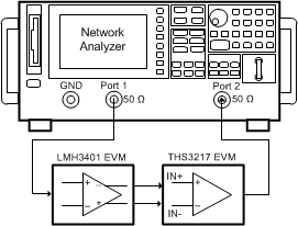 Figure 68. Frequency-Response Measurement: D2S and Full-Path (D2S + OPS) Circuit Configurations
The LMH3401 provides 7-GHz bandwidth with 0.1-dB flatness through 700 MHz. From the single-ended matched input (using active match through an internal 12.5-Ω resistor), the LMH3401 produces a differential output with 16-dB gain to the internal output pins. Building out to a 50-Ω source by adding external 40.2-Ω resistors on both differential outputs in series with the internal 10-Ω resistor, results in a net gain of 10 dB to the matched 50-Ω load on the THS3217EVM.
The maximum output swing test for the D2S stage is 4 VPP (see Figure 15 and Figure 16). With a fixed gain of 2 V/V, the tests in Figure 15 and Figure 16 require a 2-VPP differential input. In order to achieve the 2-VPP differential swing at the D2S inputs, the LMH3401 internal outputs must drive a 4-VPP differential signal around the VOCM of the LMH3401. This LMH3401 single-to-differential preamplifier is normally operated with ±2.5-V supplies, and VOCM set to ground. Under these conditions, the LMH3401 supports ±1.4 V on each internal output pin; well beyond the maximum required for THS3217 D2S characterization of ±1 V.
The output of the LMH3401EVM connects directly to the Vin+ (J1) and Vin- (J2) SMA connectors on the THS3217EVM, as shown in Figure 67. The physical spacing of the SMA connectors has been set to line up for a direct (no cabling) connection between the two different EVMs using SMA barrels. For THS3217 designs that must be evaluated before any DAC connection, consider using the LMH3401EVM as a gain of 10 dB, single-to-differential interface to the inputs of the D2S stage. This setup allows single-ended sources to generate differential output signals through the combined LMH3401EVM to THS3217EVM configuration. The D2S, small-signal, frequency-response curves over input common-mode voltage (see Figure 13) were generated by adjusting the LMH3401 voltage supplies and maintaining VOCM at midsupply to preserve input headroom on the LMH3401. In order to make single-ended, frequency-response measurements, the configuration shown in Figure 69 was used.
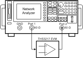 Figure 69. Frequency-Response Measurement: OPS Inverting and Noninverting, Midscale Buffer, and VREF Circuit Configurations
8.3 Harmonic Distortion Measurement
The distortion plots for all stages used a filtered high-frequency function generator to generate a very low-distortion input signal. The LMH3401 interface was used when testing the D2S and the full-signal path (D2S+OPS) harmonic distortion performance. Running the filtered signal through the LMH3401, as shown in Figure 70, provided adequate input signal purity because of the approximately –100-dBc harmonic distortion performance through 100 MHz. In order to test the harmonic-distortion performance of the OPS and midscale buffer, the configuration shown in Figure 71 was used.
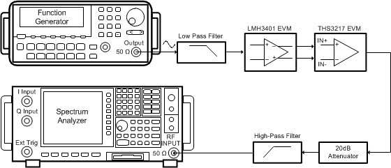 Figure 70. Harmonic-Distortion Measurement: D2S and Full-Path (D2S + OPS) Circuit Configurations
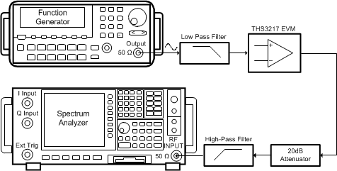 Figure 71. Harmonic-Distortion Measurement: OPS Inverting and Noninverting and Midscale Buffer Circuit Configurations
8.4 Noise Measurement
All the noise measurements were made using a very low-noise, high-gain bandwidth LMH6629 as a low-noise preamplifier to boost the output noise from the THS3217 before measurement on a spectrum analyzer, as shown in Figure 72. The 0.69-nV/√Hz input-voltage noise specification of the LMH6629 provides flat gain of 20 V/V through 100 MHz with its ultrahigh, 6.3-GHz gain bandwidth product. The D2S and OPS noise was measured with the common-mode voltage at GND.
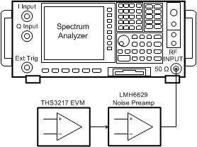 Figure 72. Noise Measurement Using LMH6629 Preamplifier
8.5 Output Impedance Measurement
Output impedance measurement for the three stages under different conditions were performed as a small-signal measurement calibrated to the device pins using an impedance analyzer. Calibrating the measurement to the device pins removes the THS3217EVM parasitic resistance, inductance, and capacitance from the measured data.
8.6 Step-Response Measurement
Generating a clean, fast, differential-input step for time-domain testing presents a considerable challenge. A multichannel pulse generator with adjustable rise and fall times was used to generate the differential pulse to drive D2S inputs in Figure 21. A high-speed scope was used to digitize the pulse response.
8.7 Feedthrough Measurement
In order to test the forward feedthrough performance of the OPS in the disabled state, the circuit shown in Figure 73 was used. The PATHSEL pin was driven low to select the internal path between the D2S and OPS. A 100-mVPP, swept-frequency, sinusoidal signal was applied at the VREF pin and the output signal was measured at the OPS output pin (VOUT). The transfer function from VREF to the output of the D2S at VO1 has a gain of 0 dB, as shown in Figure 23. The results shown in Figure 57 account for the 6-dB loss due to the doubly-terminated OPS output, and therefore report the forward feedthrough between VOUT and VO1 at different OPS gains. The D2S inputs were grounded through 50-Ω resistors for this test.
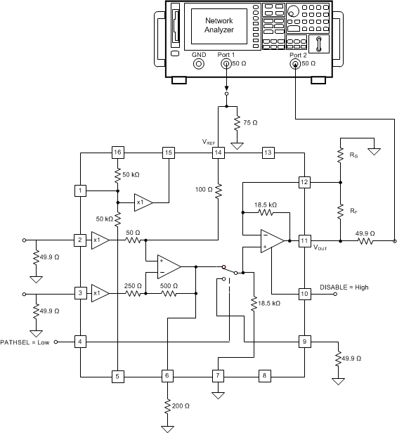 Figure 73. Forward-Feedthrough Test Circuit
In order to test the reverse feedthrough performance of the OPS in its disabled state, the circuit shown in Figure 74 was used. The PATHSEL pin was driven high to select the external path to the OPS noninverting pin, VIN+. A 100-mVPP, swept-frequency, sinusoidal signal was applied at the VIN+ pin and the output signal was measured at the D2S output pin (VO1). The results shown in Figure 58 account for the 16.5-dB loss due to the D2S termination, and the test reports the reverse feedthrough between the VO1 and VIN+ pins. The D2S inputs were grounded through 50-Ω resistors for this test.
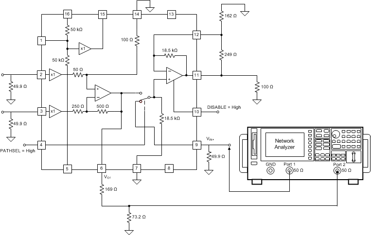 Figure 74. Reverse-Feedthrough Test Circuit
8.8 Midscale Buffer ROUT Versus CLOAD Measurement
For the tests in Figure 53 and Figure 54, the circuit shown in Figure 75 was used. The 150-Ω load circuit configured as shown, provides a 50-Ω path from the network analyzer back to the output of the buffer. As shown in Figure 75, place ROUT below the load capacitor to improve the phase margin for the closed-loop buffer output, while adding 0-Ω dc impedance into the line connected to the VREF pin.
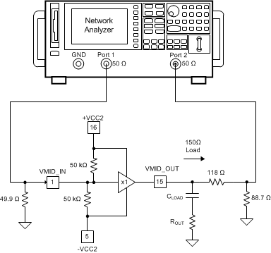 Figure 75. RS Versus CLOAD Measurement Circuit