SLOS454I January   2005  – July 2016 THS4509

PRODUCTION DATA.  

  1. Features
  2. Applications
  3. Description
  4. Revision History
  5. Device Comparison Table
  6. Pin Configuration and Functions
  7. Specifications
    1. 7.1 Absolute Maximum Ratings
    2. 7.2 ESD Ratings
    3. 7.3 Recommended Operating Conditions
    4. 7.4 Thermal Information
    5. 7.5 Electrical Characteristics: VS+ - VS- = 5 V
    6. 7.6 Electrical Characteristics: VS+ - VS- = 3 V
    7. 7.7 Dissipation Ratings
    8. 7.8 Typical Characteristics
      1. 7.8.1 Typical Characteristics: VS+ - VS- = 5 V
      2. 7.8.2 Typical Characteristics: VS+ - VS- = 3 V
  8. Detailed Description
    1. 8.1 Overview
    2. 8.2 Functional Block Diagram
    3. 8.3 Feature Description
      1. 8.3.1 Test Circuits
        1. 8.3.1.1 Frequency Response
        2. 8.3.1.2 Distortion and 1-dB Compression
        3. 8.3.1.3 S-Parameter, Slew Rate, Transient Response, Settling Time, Output Impedance, Overdrive, Output Voltage, Turnon, and Turnoff Time
        4. 8.3.1.4 CM Input
        5. 8.3.1.5 CMRR and PSRR
    4. 8.4 Device Functional Modes
  9. Application and Implementation
    1. 9.1 Application Information
    2. 9.2 Typical Applications
      1. 9.2.1 Differential Input to Differential Output Amplifier
        1. 9.2.1.1 Design Requirements
        2. 9.2.1.2 Detailed Design Procedure
          1. 9.2.1.2.1 Input Common-Mode Voltage Range
          2. 9.2.1.2.2 Setting the Output Common-Mode Voltage
          3. 9.2.1.2.3 Single-Supply Operation (3 V to 5 V)
          4. 9.2.1.2.4 THS4509 and ADS5500 Combined Performance
          5. 9.2.1.2.5 THS4509 and ADS5424 Combined Performance
        3. 9.2.1.3 Application Curve
      2. 9.2.2 Single-Ended Input to Differential Output Amplifier
  10. 10Power Supply Recommendations
  11. 11Layout
    1. 11.1 Layout Guidelines
      1. 11.1.1 General Guidelines
      2. 11.1.2 PowerPAD PCB Layout Considerations
    2. 11.2 Layout Example
    3. 11.3 PowerPAD Design Considerations
  12. 12Device and Documentation Support
    1. 12.1 Device Support
    2. 12.2 Documentation Support
      1. 12.2.1 Related Documentation
    3. 12.3 Receiving Notification of Documentation Updates
    4. 12.4 Community Resources
    5. 12.5 Trademarks
    6. 12.6 Electrostatic Discharge Caution
    7. 12.7 Glossary
  13. 13Mechanical, Packaging, and Orderable Information

Package Options

Mechanical Data (Package|Pins)
Thermal pad, mechanical data (Package|Pins)
Orderable Information

6 Pin Configuration and Functions

RGT Package
16-Pin VQFN
Top View
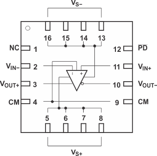
THS4509 po_los454.gif

Pin Functions

PIN TYPE DESCRIPTION
NAME NO.
NC 1 N/A No internal connection
VIN– 2 I Inverting amplifier input
VOUT+ 3 O Noninverting amplifier output
CM 4, 9 I Common-mode voltage input
VS+ 5-8 P Positive amplifier power-supply input
VOUT– 10 O Inverted amplifier output
VIN+ 11 I Noninverting amplifier input
PD 12 I Power-down; PD = logic low puts part into low power mode, PD = logic high or open for normal operation
VS– 13, 14, 15, 16 P Negative amplifier power-supply input