SLOS375B August 2014 – February 2024 THS4541
PRODUCTION DATA
- 1
- 1 Features
- 2 Applications
- 3 Description
- 4 Device Comparison Table
- 5 Pin Configuration and Functions
-
6 Specifications
- 6.1 Absolute Maximum Ratings
- 6.2 ESD Ratings
- 6.3 Recommended Operating Conditions
- 6.4 Thermal Information
- 6.5 Electrical Characteristics: (Vs+) – Vs– = 5 V
- 6.6 Electrical Characteristics: (Vs+) – Vs– = 3 V
- 6.7 Typical Characteristics 5-V Single Supply
- 6.8 Typical Characteristics: 3-V Single Supply
- 6.9 Typical Characteristics: 3-V to 5-V Supply Range
-
7 Parameter Measurement Information
- 7.1 Example Characterization Circuits
- 7.2 Frequency-Response Shape Factors
- 7.3 I/O Headroom Considerations
- 7.4 Output DC Error and Drift Calculations and the Effect of Resistor Imbalances
- 7.5 Noise Analysis
- 7.6 Factors Influencing Harmonic Distortion
- 7.7 Driving Capacitive Loads
- 7.8 Thermal Analysis
-
8 Detailed Description
- 8.1 Overview
- 8.2 Functional Block Diagram
- 8.3 Feature Description
- 8.4
Device Functional Modes
- 8.4.1
Operation from Single-Ended Sources to Differential Outputs
- 8.4.1.1 AC-Coupled Signal Path Considerations for Single-Ended Input to Differential Output Conversion
- 8.4.1.2 DC-Coupled Input Signal Path Considerations for Single-Ended to Differential Conversion
- 8.4.1.3 Resistor Design Equations for the Single-Ended to Differential Configuration of the FDA
- 8.4.1.4 Input Impedance for the Single-Ended to Differential FDA Configuration
- 8.4.2 Differential-Input to Differential-Output Operation
- 8.4.1
Operation from Single-Ended Sources to Differential Outputs
- 9 Application and Implementation
- 10Device and Documentation Support
- 11Revision History
- 12Mechanical, Packaging, and Orderable Information
Package Options
Refer to the PDF data sheet for device specific package drawings
Mechanical Data (Package|Pins)
- RUN|10
- RGT|16
Thermal pad, mechanical data (Package|Pins)
Orderable Information
7.2 Frequency-Response Shape Factors
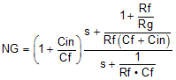
Figure 6-1 illustrates the small-signal response shape versus gain using a fixed 402-Ω feedback resistor in the circuit of Figure 7-1. Being a voltage-feedback based FDA, the THS4541 shows a response shape that varies with gain setting, largely determined by the loop-gain crossover frequency and phase margin at the crossover. This loop-gain crossover frequency is where the open-loop response and the noise gain intersect (where the loop gain drops to 1). The noise gain is the inverse of the voltage divider from the outputs back to the differential inputs; use a balanced divider ratio on each feedback path. In general, the noise gain (NG) does not equal the signal gain for designs providing an input match from a source impedance. NG is given by 1 + Rf / (total impedance from the inverting summing junction to ground). Using the resistor values computed in the gain sweep of Table 8-1, and repeating that sweep showing the NG gives Table 7-1, where only the exact R solutions are shown.
| SIGNAL GAIN | Rt, EXACT (Ω) | Rg1, EXACT (Ω) | Rg2, EXACT (Ω) | NOISE GAIN |
|---|---|---|---|---|
| 1 | 55.2 | 399 | 425 | 1.94 |
| 2 | 60.1 | 191 | 218 | 2.85 |
| 3 | 65.6 | 124 | 153 | 3.63 |
| 4 | 72 | 89.7 | 119 | 4.37 |
| 5 | 79.7 | 67.8 | 98.3 | 5.09 |
| 6 | 89.1 | 54.2 | 86.5 | 5.65 |
| 7 | 101 | 43.2 | 76.6 | 6.25 |
| 8 | 117 | 35.2 | 70.1 | 6.74 |
| 9 | 138 | 29 | 65.8 | 7.11 |
| 10 | 170 | 23.6 | 62.5 | 7.44 |
| 11 | 220 | 18.7 | 59.3 | 7.78 |
| 12 | 313 | 14.6 | 57.7 | 7.97 |
| 13 | 545 | 10.8 | 56.6 | 8.11 |
| 14 | 2209 | 7.26 | 56.1 | 8.16 |
NG is critically important for bandwidth and all output error terms (such as dc offset and noise). For lower-speed devices, normally only the dc noise gain is considered. However, for the THS4541, with loop gain crossover at greater than 300 MHz, the feedback network produces a parasitic pole to the differential summing junctions that causes the noise gain to increase with frequency. This pole causes a lower than expected crossover frequency added phase shift around the loop. Consider the feedback network (single-ended) of Figure 7-5, showing a parasitic 0.2 pF on the feedback 402 Ω resistor. The 0.85 pF differential input capacitance of the THS4541 is converted to single-ended as a 1.7 pF parasitic for this single-sided analysis circuit (the Rg shown is Rg2 in Figure 7-1).
 Figure 7-5 Feedback Network for the
Gain of 2 Configuration Using 402 Ω and Matching
to a 50 Ω Source
Figure 7-5 Feedback Network for the
Gain of 2 Configuration Using 402 Ω and Matching
to a 50 Ω SourceThe response shape from Vout to Vin in Figure 7-5 has a pole and then a zero. To describe NG, invert the Laplace transform of Vin and Vout from Figure 7-5 to provide the frequency-dependent NG response of Equation 1, where a zero comes in first and then a pole.
The zero location is key. Using the gain of 2 values of Figure 7-5, the estimated zero in the NG is 588 MHz. Limiting the parasitic capacitance at the summing junctions, either differentially or signal-ended, to a ground or power plane is critical in board layouts.
Using this feedback model, and the open-loop gain and phase data for the THS4541, allows the Aol and NG curves over frequency to be drawn, as shown in Figure 7-6, where the peaking in the noise gain pulls the intersection point back in frequency.
 Figure 7-6 Aol and Noise Gain Plots for the Lower Gains of Figure 7-1
To assess closed-loop bandwidth and peaking, the noise-gain phase must be subtracted from the THS4541 Aol phase to obtain the total phase around the loop, as shown in Figure 7-7.
 Figure 7-7 Loop-Gain Phase for the
Three Lower Gains of Figure 6-1
Figure 7-7 Loop-Gain Phase for the
Three Lower Gains of Figure 6-1From Figure 7-6 and Figure 7-7, using Table 7-2, tabulate the loop-gain crossover frequency and phase margin at these crossovers to explain the response shapes of Figure 6-1.
| GAIN | DC NG (V/V) | 0-dB LG (MHz) | PHASE MARGIN (°) |
|---|---|---|---|
| 0.1 | 1.1 | 457 | 18 |
| 1 | 1.94 | 380 | 41 |
| 2 | 2.85 | 302 | 59 |
From these crossover (or 0-dB loop gain) frequencies, a good approximation for the resulting f–3dB is to multiply the crossover frequencies by 1.6 when the phase margin is less than 65°. Ideally, a 65° phase margin at loop-gain crossover provides a flat Butterworth closed-loop response. The 59° phase margin for the gain of 2 setting explains the nearly flat response for this condition with 1.6 × 302 MHz = 483 MHz, estimated with f–3dB closely matching the measured 500-MHz SSBW.
The very low phase margin in the attenuator setting at 0.1 V/V explains the highly peaked response in Figure 6-1. This peaking can be easily compensated, as shown in Section 9.2.1, using feedback capacitors and a differential capacitor across the inputs.
Considering the noise gain zero as part of the loop-gain analysis shows the importance of using relatively-low, feedback-resistor values and minimizing layout parasitic capacitance on the input pins of the THS4541 to reduce the effects of this feedback pole. The TINA model does a good job of predicting these issues (the model includes the 0.85 pF differential internal capacitance); add any estimated external parasitic capacitance on the summing junctions in simulation to predict the response shape more accurately.