SLOS375B August 2014 – February 2024 THS4541
PRODUCTION DATA
- 1
- 1 Features
- 2 Applications
- 3 Description
- 4 Device Comparison Table
- 5 Pin Configuration and Functions
-
6 Specifications
- 6.1 Absolute Maximum Ratings
- 6.2 ESD Ratings
- 6.3 Recommended Operating Conditions
- 6.4 Thermal Information
- 6.5 Electrical Characteristics: (Vs+) – Vs– = 5 V
- 6.6 Electrical Characteristics: (Vs+) – Vs– = 3 V
- 6.7 Typical Characteristics 5-V Single Supply
- 6.8 Typical Characteristics: 3-V Single Supply
- 6.9 Typical Characteristics: 3-V to 5-V Supply Range
-
7 Parameter Measurement Information
- 7.1 Example Characterization Circuits
- 7.2 Frequency-Response Shape Factors
- 7.3 I/O Headroom Considerations
- 7.4 Output DC Error and Drift Calculations and the Effect of Resistor Imbalances
- 7.5 Noise Analysis
- 7.6 Factors Influencing Harmonic Distortion
- 7.7 Driving Capacitive Loads
- 7.8 Thermal Analysis
-
8 Detailed Description
- 8.1 Overview
- 8.2 Functional Block Diagram
- 8.3 Feature Description
- 8.4
Device Functional Modes
- 8.4.1
Operation from Single-Ended Sources to Differential Outputs
- 8.4.1.1 AC-Coupled Signal Path Considerations for Single-Ended Input to Differential Output Conversion
- 8.4.1.2 DC-Coupled Input Signal Path Considerations for Single-Ended to Differential Conversion
- 8.4.1.3 Resistor Design Equations for the Single-Ended to Differential Configuration of the FDA
- 8.4.1.4 Input Impedance for the Single-Ended to Differential FDA Configuration
- 8.4.2 Differential-Input to Differential-Output Operation
- 8.4.1
Operation from Single-Ended Sources to Differential Outputs
- 9 Application and Implementation
- 10Device and Documentation Support
- 11Revision History
- 12Mechanical, Packaging, and Orderable Information
Package Options
Refer to the PDF data sheet for device specific package drawings
Mechanical Data (Package|Pins)
- RUN|10
- RGT|16
Thermal pad, mechanical data (Package|Pins)
Orderable Information
7.1 Example Characterization Circuits
The THS4541 offers the advantages of a fully differential amplifier (FDA) design, with the trimmed input offset voltage of a precision op amp. The FDA is an extremely flexible device that provides a purely differential output signal centered on a settable output common-mode level. The primary options revolve around the choices of single-ended or differential inputs, ac-coupled or dc-coupled signal paths, gain targets, and resistor-value selections. Figure 6-1 to Figure 6-36 shows the characterizations that focus on single-ended-to-differential designs as the more challenging application requirement. Differential sources can certainly be supported and are often simpler to implement and analyze.
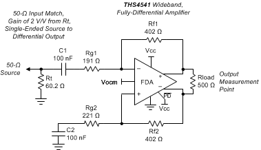
Because most lab equipment is single-ended, the characterization circuits typically operate with a single-ended, matched, 50-Ω input termination to a differential output at the FDA output pins. That output is then translated back to single-ended through a variety of baluns (or transformers) depending on the test and frequency range. DC-coupled, step-response testing uses two 50-Ω scope inputs with trace math. Figure 7-1 shows the starting point for any single-ended-to-differential, ac-coupled characterization plot.
 Figure 7-1 AC-Coupled, Single-Ended Source to a
Differential Gain of a 2 V/V Test Circuit
Figure 7-1 AC-Coupled, Single-Ended Source to a
Differential Gain of a 2 V/V Test CircuitFigure 7-1 shows how most characterization plots fix the Rf (Rf1 = Rf2) value at 402 Ω. This element value is completely flexible in application, but the 402 Ω provides a good compromise for the parasitic issues linked to this value, specifically:
- Added output loading. The FDA appears like an inverting op amp design with both feedback resistors as an added load across the outputs. Figure 7-1 shows how the approximate total differential load is 500 Ω || 804 Ω = 308 Ω.
- Noise contributions because of the resistor values. The resistors contribute both a 4kTR term and provide gain for the input current noise (see Section 7.5).
- Parasitic feedback pole at the input summing
nodes. This pole created by the feedback R value and the
0.85 pF differential input capacitance (as well as any board layout parasitic) introduces a zero in the noise gain, decreasing the phase margin in most situations. This effect must be managed for best frequency response flatness or step response overshoot. The 402 Ω value selected does degrade the phase margin slightly over a lower value, but does not decrease the loading significantly from the nominal 500 Ω value across the output pins.
Figure 7-1 shows the starting selections for the frequency domain characterization curves. Then, various elements are modified to show the impact over a range of design targets, specifically:
- Gain setting is changed by adjusting Rt and the 2 – Rg elements (holding a 50-Ω input match).
- Output loading, including both resistive and capacitive load testing.
- Power-supply settings. Most often, a single +5-V test uses a ±2.5-V supply, and a +3-V test uses ±1.5-V supplies.
- The disable control pin is tied to Vs+ for any active channel test.
Because most network and spectrum analyzers are a single-ended input, the output network on the THS4541 characterization tests typically show the desired load connected through a balun to a single-ended, 50-Ω load, while presenting a 50-Ω source from the balun output back into the balun. For instance, Figure 7-2 shows a wideband MA/Com balun used for Figure 7-1. This network shows a 500-Ω differential load to the THS4541, but an ac-coupled, 50-Ω source to the network analyzer. Distortion testing typically uses a lower-frequency, dc-isolated balun (such as the TT1-6T) that is rotated 90° from the wider band interface of Figure 7-2.
 Figure 7-2 Example 500-Ω Load to a Single-Ended,
Doubly-Terminated, AC-Coupled, 50-Ω Interface
Figure 7-2 Example 500-Ω Load to a Single-Ended,
Doubly-Terminated, AC-Coupled, 50-Ω InterfaceThis approach allows a higher differential load, but with a wideband 50-Ω output match at the cost of considerable signal-path insertion loss. This loss is acceptable for characterization, and is normalized out to show the characterization curves.
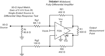
Figure 7-3 shows the circuit that is used as a starting point for time-domain or dc-coupled testing, where the gain of a 5 V/V setting used in Figure 6-25 and Figure 6-27 are illustrated.
 Figure 7-3 DC-Coupled, Single-Ended-to-Differential, Basic
Test Circuit Set for a Gain of 5 V/V
Figure 7-3 DC-Coupled, Single-Ended-to-Differential, Basic
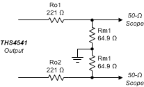
Test Circuit Set for a Gain of 5 V/VIn this case, the input is dc-coupled, showing a 50-Ω input match to the source, having a gain of 5 V/V to a differential output, and again is driving a nominal 500-Ω load. Using a single supply, the Vocm control input can either be floated (defaulting to mid-supply) or be driven within the allowed range for the Vocm loop (see the headroom limits on Vocm in the Electrical Characteristics tables). To use this circuit for step-response measurements, load each of the two outputs with a 250-Ω network, translating to a 50-Ω source impedance driving into two 50-Ω scope inputs. Then, difference the scope inputs to generate the step responses of Figure 6-9 and Figure 6-27. Figure 7-4 shows the output interface circuit. This grounded interface pulls a dc load current from the output Vocm voltage for single-supply operation. Running this test with balanced bipolar power supplies eliminates this dc load current and gives similar waveform results.
 Figure 7-4 Example 500-Ω Load to Differential,
Doubly-Terminated, DC-Coupled 50-Ω Scope Interface