SLOS375B August 2014 – February 2024 THS4541
PRODUCTION DATA
- 1
- 1 Features
- 2 Applications
- 3 Description
- 4 Device Comparison Table
- 5 Pin Configuration and Functions
-
6 Specifications
- 6.1 Absolute Maximum Ratings
- 6.2 ESD Ratings
- 6.3 Recommended Operating Conditions
- 6.4 Thermal Information
- 6.5 Electrical Characteristics: (Vs+) – Vs– = 5 V
- 6.6 Electrical Characteristics: (Vs+) – Vs– = 3 V
- 6.7 Typical Characteristics 5-V Single Supply
- 6.8 Typical Characteristics: 3-V Single Supply
- 6.9 Typical Characteristics: 3-V to 5-V Supply Range
-
7 Parameter Measurement Information
- 7.1 Example Characterization Circuits
- 7.2 Frequency-Response Shape Factors
- 7.3 I/O Headroom Considerations
- 7.4 Output DC Error and Drift Calculations and the Effect of Resistor Imbalances
- 7.5 Noise Analysis
- 7.6 Factors Influencing Harmonic Distortion
- 7.7 Driving Capacitive Loads
- 7.8 Thermal Analysis
-
8 Detailed Description
- 8.1 Overview
- 8.2 Functional Block Diagram
- 8.3 Feature Description
- 8.4
Device Functional Modes
- 8.4.1
Operation from Single-Ended Sources to Differential Outputs
- 8.4.1.1 AC-Coupled Signal Path Considerations for Single-Ended Input to Differential Output Conversion
- 8.4.1.2 DC-Coupled Input Signal Path Considerations for Single-Ended to Differential Conversion
- 8.4.1.3 Resistor Design Equations for the Single-Ended to Differential Configuration of the FDA
- 8.4.1.4 Input Impedance for the Single-Ended to Differential FDA Configuration
- 8.4.2 Differential-Input to Differential-Output Operation
- 8.4.1
Operation from Single-Ended Sources to Differential Outputs
- 9 Application and Implementation
- 10Device and Documentation Support
- 11Revision History
- 12Mechanical, Packaging, and Orderable Information
Package Options
Refer to the PDF data sheet for device specific package drawings
Mechanical Data (Package|Pins)
- RUN|10
- RGT|16
Thermal pad, mechanical data (Package|Pins)
Orderable Information
8.4.2.1 AC-Coupled, Differential-Input to Differential-Output Design Issues
There are two typical ways to use the THS4541 with an ac-coupled differential source. In the first method, the source is differential and can be coupled in through two blocking capacitors. The second method uses either a single-ended or a differential source and couples in through a transformer (or balun). Figure 8-2 shows a typical blocking capacitor approach to a differential input. An optional input differential termination resistor (Rm) is included in this design. This Rm element allows the input Rg resistors to be scaled up while still delivering lower differential input impedance to the source. In this example, the Rg elements sum to show a 200-Ω differential impedance, while the Rm element combines in parallel to give a net 100-Ω, ac-coupled, differential impedance to the source. Again, the design proceeds ideally by selecting the Rf element values, then the Rg to set the differential gain, then an Rm element (if needed) to achieve a target input impedance. Alternatively, the Rm element can be eliminated, the Rg elements set to the desired input impedance, and Rf set to the get the differential gain (= Rf / Rg).
 Figure 8-2 Example Down-Converting Mixer Delivering an
AC-Coupled Differential Signal to the THS4541
Figure 8-2 Example Down-Converting Mixer Delivering an
AC-Coupled Differential Signal to the THS4541The dc biasing here is very simple. The output Vocm is set by the input control voltage and, because there is no dc current path for the output common-mode voltage, that dc bias also sets the input pins common-mode operating points.
Transformer input coupling allows either a single-ended or differential source to be coupled into the THS4541; possibly also improving the input-referred noise figure. These designs assume a source impedance that must be matched in the balun interface. The simplest approach is shown in Figure 8-3, where an example 1:2 turns ratio step-up transformer is used from a 50-Ω source.
 Figure 8-3 Input Balun Interface Delivers a Differential
Input to the THS4541
Figure 8-3 Input Balun Interface Delivers a Differential
Input to the THS4541In this example, this 1:2 turns ratio step-up transformer provides a source and load match from the 50-Ω source if the secondary is terminated in 200 Ω (turns-ratio squared is the impedance ratio across a balun). The two Rg elements provide that termination as the elements sum to the differential virtual ground at the FDA summing junctions. The input blocking cap (C1) is optional and included only to eliminate dc shorts to ground from the source. This solution often improves the input-referred noise figure more so than just the FDA using this passive (zero power dissipation) input balun. Defining a few ratios allows a noise figure expression to be written as Equation 14:
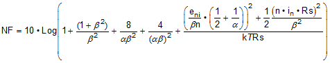
where
- n ≡ turns ratio (the ohms ratio is then n2)
- α ≡ differential gain in the FDA = Rf / Rg
- β ≡ transformer insertion loss in V/V (from a dB insertion loss, convert to linear attenuation = β)
- kT = 4e-21J at 290 K (17°C)
One way to use Equation 14 is to fix the input balun selection, and then sweep the FDA gain by stepping up the Rf value. The lowest-noise method uses just the two Rg elements for termination matching (no Rm element, such as in Figure 8-3) and sweep the Rf values up to assess the resulting input-referred noise figure. While this method can be used with all FDAs and a wide range of input baluns, relatively low-frequency input baluns are an appropriate choice here because the THS4541 holds exceptional SFDR for less than 40-MHz applications. Two representative selections, with typical measured spans and resulting model elements, are shown in Table 8-2. For these two selections, the critical inputs for the noise figures are the turns ratio and the insertion loss (the 0.2 dB for the CX2014LNL becomes a β = 0.977 in the NF expression).
| PART NUMBER | Rs (Ω) | –1-dB FREQUENCY (MHz) | INSERTION LOSS (dB) | MFR | NO. OF DECADES | –3-dB FREQUENCY (MHz) | TURNS RATIO | MODEL ELEMENTS | ||||||
|---|---|---|---|---|---|---|---|---|---|---|---|---|---|---|
| MIN | MAX | –1-dB POINTS | –3-dB POINTS | MIN | MAX | L1 (µH) | L2 (µH) | k | M (µH) | |||||
| ADT2-1T | 50 | 0.1 | 463 | 0.3 | MiniCircuits | 3.67 | 4.22 | 0.05 | 825 | 1.41 | 79.57747 | 158.50797 | 0.99988 | 112.19064 |
| CX2047LNL | 50 | 0.083 | 270 | 0.2 | Pulse Eng | 3.51 | 3.93 | 0.044 | 372 | 2 | 90.42894 | 361.71578 | 0.99976 | 180.81512 |
Using the typical input referred noise terms for the THS4541 (eni = 2.2 nV and in = 1.9 pA) and sweeping the total gain from the input of the balun to the differential output over a 10-dB to 24-dB span, gives the input noise figure shown in Figure 8-4.
 Figure 8-4 Noise Figure versus Total Gain with the Two Input Baluns of Table 8-2
The 50-Ω referred noise figure estimates show a
decreasing input-referred noise for either balun as the gain increases through 24 dB. To
achieve the total target gain after the step up from the input balun, the only elements
changing in these sweeps are the feedback-resistor values. The example of Figure 8-3 is a gain of
7.86 V/V, or a 17.9-dB gain where a 9.0-dB
input noise figure is predicted from Figure 8-4. Another advantage for this method is that the effective noise gain (NG) is reduced by
the source impedance appearing as part of the total Rg element in the design. The example of
Figure 8-3 operates with a NG = 1 + 402 / (100 + 100) = 3 V/V, giving greater than 300-MHz SSBW in
the THS4541 portion of the design. Combining that capability with the 372
MHz in the balun gives greater than 200 MHz in this 18-dB gain stage; or an equivalent
greater than 1.6-GHz gain bandwidth product in a low-power, high dynamic range
interface.
Added features and considerations for the balun input of Figure 8-3 include:
- Many of these baluns offer a secondary centertap. Leave the centertap unconnected for the best HD2 suppression and DC biasing (do not include a capacitor from this centertap to ground).
- With a floating secondary centertap, the input pins common-mode voltage again equals the output Vocm setting because there is no DC path for the output common-mode voltage to create a common-mode current (ICM).