SLES032E June 2002 – September 2014 THS8200
PRODUCTION DATA.
- 1 Device Overview
- 2 Revision History
- 3 Terminal Configuration and Functions
-
4 Specifications
- 4.1 Absolute Maximum Ratings
- 4.2 Handling Ratings
- 4.3 Recommended Operating Conditions
- 4.4 Power Consumption Summary
- 4.5 Power Supply
- 4.6 Digital Inputs, DC Characteristics
- 4.7 Analog (DAC) Outputs
- 4.8 Nonlinearity
- 4.9 Analog Output Bandwidth (sinx/x corrected) at fS = 205 MSPS
- 4.10 Output Compliance vs Full-Scale Adjustment Resistor Value
- 4.11 Vertical Sync of the HDTV 1080I Format Preset in First and Second Field, and Horizontal Line Waveform Detail
-
5 Functional Overview
- 5.1
Data Manager (DMAN)
- 5.1.1 Interpolating Finite Impulse Responses Filter (IFIR)
- 5.1.2 Color-Space Conversion (CSC)
- 5.1.3 Clip/Shift/Multiplier (CSM)
- 5.1.4 Digital Multiplexer (DIGMUX)
- 5.1.5 Display Timing Generator (DTG)
- 5.1.6 Clock Generator (CGEN)
- 5.1.7 Clock Driver (CDRV)
- 5.1.8 I2C Host Interface (I2CSLAVE)
- 5.1.9 Test Block (TST)
- 5.1.10 D/A Converters (DACs)
- 5.1
Data Manager (DMAN)
-
6 Detailed Functional Description
- 6.1 Data Manager (DMAN)
- 6.2 Input Interface Formats
- 6.3 Clock Generator (CGEN)/Clock Driver (CDRV)
- 6.4 Color Space Conversion (CSC)
- 6.5 Clip/Shift/Multiplier (CSM)
- 6.6 Interpolating Finite Impulse Response Filter (IFIR)
- 6.7
Display Timing Generator (DTG)
- 6.7.1 Overview of Functionality
- 6.7.2 Functional Description
- 6.7.3
DTG Line Type Overview
- 6.7.3.1 HDTV Mode
- 6.7.3.2 Active Video
- 6.7.3.3 FULL NTSP (Full Normal Tri-Level Sync Pulse)
- 6.7.3.4 NTSP NTSP (Normal Tri-Level Sync Pulse/Normal Tri-Level Sync Pulse)
- 6.7.3.5 BTSP BTSP (Broad Pulse and Tri-Level Sync Pulse/Broad Pulse and Tri-Level Sync Pulse)
- 6.7.3.6 NTSP BTSP (Normal Tri-Level Sync Pulse/ Broad Pulse and Tri-Level Sync Pulse)
- 6.7.3.7 BTSP NTSP (Broad Pulse and Tri-Level Sync Pulse/Normal Tri-Level Sync Pulse)
- 6.7.3.8 Full BTSP (Full Broad Pulse and Tri-Level Sync Pulse)
- 6.7.3.9 SDTV Mode
- 6.7.3.10 NEQ_NEQ (Negative Equalization Pulse/Negative Equalization Pulse)
- 6.7.3.11 FULL_BSP (Full Broad Sync Pulse)
- 6.7.3.12 BSP_BSP (Broad Sync Pulse/Broad Sync Pulse)
- 6.7.3.13 FULL_NSP (Full Normal Sync Pulse)
- 6.7.3.14 NEQ_BSP (Negative Equalization Pulse/Broad Sync Pulse)
- 6.7.3.15 BSP_NEQ (Broad Sync Pulse/Negative Equalization Pulse)
- 6.7.3.16 FULL_NEQ (Full Negative Equalization Pulse)
- 6.7.3.17 NSP_ACTIVE (Normal Sync Pulse/Active Video)
- 6.7.3.18 ACTIVE_NEQ (Active Video/Negative Equalization Pulse)
- 6.7.3.19 ACTIVE VIDEO
- 6.8
D/A Conversion
- 6.8.1 RGB Output Without Sync Signal Insertion/General-Purpose Application DAC
- 6.8.2 SMPTE-Compatible RGB Output With Sync Signal Inserted on G (Green) Channel
- 6.8.3 SMPTE-Compatible Analog-Level Output With Sync Inserted on All RGB Channels
- 6.8.4 SMPTE-Compatible YPbPr Output With Sync Signal Inserted on Y Channel Only
- 6.8.5 SMPTE-Compatible YPbPr Output With Sync Signal Inserted on All Channels
- 6.8.6 Summary of Supported Video Formats
- 6.9 Test Functions
- 6.10 Power Down
- 6.11 CGMS Insertion
- 6.12 I2C Interface
-
7 I2C Registers
- 7.1 I2C Register Map
- 7.2
Register Descriptions
- 7.2.1 System Control (Sub-Addresses 0x02−0x03)
- 7.2.2 Color Space Conversion Control (Sub-Addresses 0x04−0x19)
- 7.2.3 Test Control (Sub-Addresses 0x1A−0x1B)
- 7.2.4 Data Path Control (Sub-Address 0x1C)
- 7.2.5 Display Timing Generator Control, Part 1 (Sub-Addresses 0x1D−0x3C)
- 7.2.6 DAC Control (Sub-Addresses 0x3D−0x40)
- 7.2.7 Clip/Shift/Multiplier Control (Sub-Addresses 0x41−0x4F)
- 7.2.8 Display Timing Generator Control, Part 2 (Sub-Addresses 0x50−0x82)
- 7.2.9 CGMS Control (Sub-Addresses 0x83−0x85)
- 7.3 THS8200 Preset Mode Line Type Definitions
- 8 Application Information
- 9 Device and Documentation Support
- 10Mechanical, Packaging, and Orderable Information
Package Options
Mechanical Data (Package|Pins)
- PFP|80
Thermal pad, mechanical data (Package|Pins)
- PFP|80
Orderable Information
8 Application Information
8.1 Video vs Computer Graphics Application
THS8200 is a highly integrated and flexible universal analog component video/graphics generator that can be used in any application requiring D/A conversion of video/graphics signals.
In a typical video application (for example, DVD player, set-top box), the THS8200 receives its input from an MPEG decoder or media processor engine and converts the signal into the analog domain, thereby generating the correct timing/frame format for the selected format.
Its ITU-R.BT656 output port could be used to connect to an NTSC/PAL video encoder, such as the Texas Instruments TVP6000, for regular composite/S-video output.
Note that because the DAC speed is rated up to 205 MSPS, all popular SDTV and HDTV formats, including 1080I and 720P, are supported in both 1x and 2x interpolated modes. The 1080P is supported at the 1x rate.
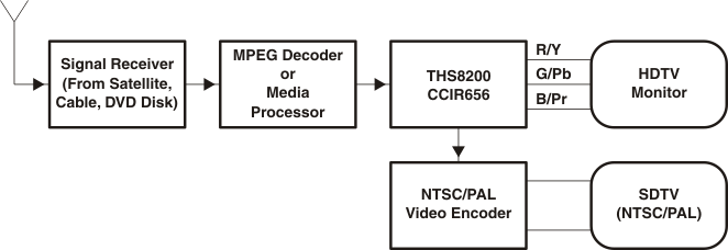 Figure 8-1 Typical Video Application
Because of its programmable Hsync/Vsync outputs, the on-chip support for RGB as well as YCbCr color spaces and its internal color space conversion circuit, and the DAC operational speed of 205 MSPS, all PC graphics formats are supported as well, up to UXGA at 75 Hz. Video interpolation is now bypassed so that the full 205 MSPS can be used for the 1x pixel clock.
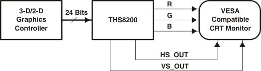 Figure 8-2 Computer Graphics Application
8.2 DVI to Analog YPbPr/RGB Application
Together with a DVI receiver, this device forms a two-chip solution to convert video or graphics formats sent over a DVI interface to an analog RGB or YPbPr format using embedded composite sync or separate Hsync, Vsync. THS8200 connects gluelessly to a DVI receiver using its data input bus and HS_IN and VS_IN terminals. TI DVI 1.0 (with HDCP) receivers provide a data enable (DE) signal that is high during the active video window. The THS8200 can be configured to interpret this DE signal on its FID terminal to automatically insert a user-programmable blanking-level amplitude outside the active video window on its analog outputs; this blanking level can be correctly positioned for either RGB or YPbPr analog outputs. The user can optionally perform color space conversion in the THS8200 and adjust offset and gain ranges through the device's CSM block.
When sending (interlaced) video over DVI, the EIA-861 specification describes a method to derive the fieldID signal—not directly available from a DVI1.0 (with HDCP) receiver—from the relative alignment of the Hsync and Vsync signals. The THS8200 can be configured to derive internally the correct even/odd field identification from Hsync/Vsync alignment according to this specification, instead of using the FieldID signal on its FID input terminal. This avoids the need for additional glue logic in a DVI application.
8.3 Master vs Slave Timing Modes
In slave timing mode, the THS8200 output display timing is synchronized to the video data source. Display timing output signals are based on input sync signals, either fed to the device on the dedicated Hsync, Vsync, and FieldID (HS_IN, VS_IN, and FID) input terminals or based on SAV/EAV codes embedded in the input video data.
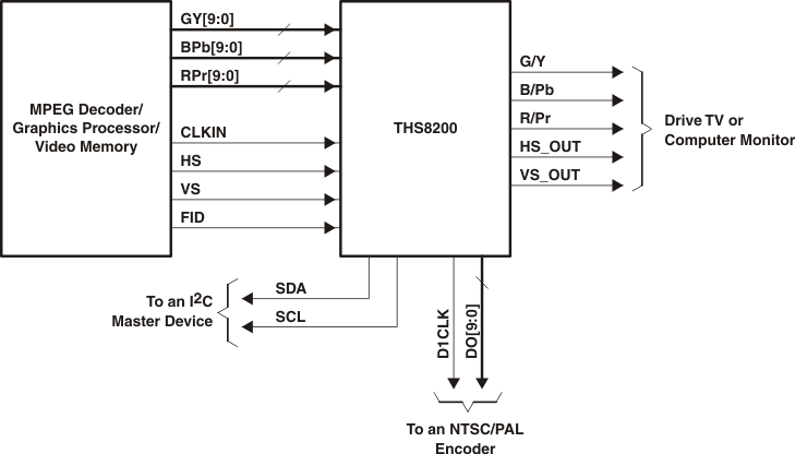 Figure 8-3 Slave Operation Mode of THS8200
In master timing mode, the THS8200 generates two sets of output synchronization signals.
- HS_IN and VS_IN now become output signals to the video source (FID unused).
- HS_OUT and VS_OUT are still output signals to display device.
The intended purpose is that THS8200 requests video data from a source that requires external timing, such as video memory.
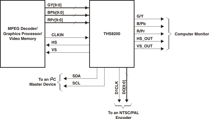 Figure 8-4 Master Operation Mode of THS8200